Rf amplifier pcb
Design Considerations for RF Amplifier PCB Layout
Designing a printed circuit board (PCB) for an RF amplifier involves a meticulous process that requires careful consideration of various factors to ensure optimal performance. The complexity of RF signals, which operate at high frequencies, necessitates a precise approach to PCB layout to minimize losses and interference.
One of the primary considerations in RF amplifier PCB design is the selection of materials.
The dielectric material used in the PCB can significantly affect signal integrity. Materials with low dielectric constant and low loss tangent are preferred as they help in reducing signal attenuation and maintaining signal speed. Additionally, the thickness of the substrate should be chosen to match the impedance requirements of the circuit.
Transitioning from material selection, the layout of the components is another critical aspect.
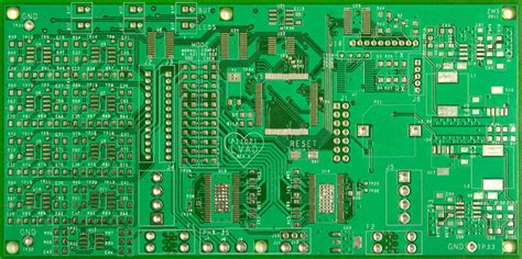
The placement of components on an RF amplifier PCB must be done with an understanding of the signal path and the need to minimize parasitic inductance and capacitance. Components should be placed as close as possible to each other to reduce the length of the signal path, which in turn minimizes the potential for signal degradation. Furthermore, the orientation of components can also impact performance; aligning components in a manner that follows the natural flow of the signal can help in maintaining signal integrity.
Moreover, grounding is a crucial element in RF amplifier PCB design.
A solid ground plane is essential to provide a return path for the signals and to minimize electromagnetic interference (EMI). The ground plane should be continuous and unbroken to ensure that it effectively shields the circuit from external noise. Additionally, the use of via stitching can enhance the performance of the ground plane by providing multiple paths for the return current, thereby reducing the potential for ground loops.
In addition to grounding, impedance matching is another vital consideration.
Impedance mismatches can lead to signal reflections, which degrade the performance of the RF amplifier. To address this, designers must carefully calculate and implement transmission lines that match the impedance of the source and load. This often involves the use of microstrip or stripline techniques, which require precise control over the width and spacing of the traces to achieve the desired impedance.
Thermal management is also an important factor in RF amplifier PCB design.
High-frequency operation can generate significant heat, which, if not properly managed, can affect the reliability and performance of the amplifier. Effective thermal management strategies include the use of thermal vias, heat sinks, and careful placement of components to ensure adequate heat dissipation.
Finally, testing and validation are essential steps in the design process.
Once the PCB is fabricated, it must be thoroughly tested to ensure that it meets the desired specifications. This involves measuring parameters such as gain, bandwidth, and noise figure to verify that the amplifier performs as expected. Any discrepancies must be addressed through iterative design adjustments and re-testing.
In conclusion, designing an RF amplifier PCB requires a comprehensive understanding of various technical considerations, from material selection and component layout to grounding, impedance matching, and thermal management. By carefully addressing each of these factors, designers can create PCBs that deliver high performance and reliability in RF applications.

Material Selection for High-Frequency RF Amplifier PCBs
When designing high-frequency RF amplifier PCBs, the selection of materials plays a crucial role in determining the performance and reliability of the final product. The choice of substrate material, in particular, can significantly impact the electrical characteristics, thermal management, and overall durability of the PCB. As such, understanding the properties and implications of various materials is essential for engineers and designers working in this field.
To begin with, the dielectric constant (Dk) of the substrate material is a primary consideration.
A lower dielectric constant is generally preferred for high-frequency applications as it reduces signal loss and allows for faster signal propagation. Materials such as PTFE (polytetrafluoroethylene), commonly known by the brand name Teflon, are often favored due to their low Dk values. However, PTFE can be challenging to work with due to its mechanical properties, necessitating careful handling and processing.
In addition to the dielectric constant, the loss tangent (also known as dissipation factor) is another critical parameter.
This factor measures the inherent energy loss of the material as the signal passes through it. For RF applications, a low loss tangent is desirable to minimize signal attenuation and maintain signal integrity. Advanced materials like Rogers RO4000 series and Taconic RF-35 are engineered to offer low loss tangents, making them suitable for high-frequency applications.
Thermal management is another vital aspect to consider when selecting materials for RF amplifier PCBs.
High-frequency operations can generate significant heat, which, if not properly managed, can lead to performance degradation or even failure. Materials with high thermal conductivity, such as ceramic-filled PTFE composites, can effectively dissipate heat, ensuring stable operation. Additionally, the coefficient of thermal expansion (CTE) should be compatible with other components to prevent mechanical stress and potential damage during temperature fluctuations.
Moreover, the mechanical properties of the substrate material should not be overlooked.
The material must provide sufficient rigidity and support to withstand the physical demands of the application. This is particularly important in environments subject to vibration or mechanical shock. Materials like FR-4, while commonly used in general PCB applications, may not always meet the stringent requirements of high-frequency RF designs due to their higher dielectric constant and loss tangent compared to specialized RF materials.
Furthermore, cost considerations often influence material selection.
While high-performance materials like PTFE and ceramic composites offer superior electrical and thermal properties, they can be significantly more expensive than standard materials like FR-4. Therefore, a balance must be struck between performance requirements and budget constraints. In some cases, hybrid constructions that combine different materials may offer a cost-effective solution without compromising on performance.
In conclusion, the selection of materials for high-frequency RF amplifier PCBs is a complex process that requires careful consideration of various factors, including dielectric properties, thermal management, mechanical strength, and cost. By understanding the trade-offs and benefits of different materials, engineers can make informed decisions that optimize the performance and reliability of their designs. As technology continues to advance, ongoing research and development in material science will likely yield new options that further enhance the capabilities of RF amplifier PCBs, paving the way for even more sophisticated and efficient electronic systems.

Thermal Management Techniques in RF Amplifier PCB Design
In the realm of RF amplifier PCB design, thermal management emerges as a critical consideration, given the significant heat generated during operation. Effective thermal management not only ensures the reliability and longevity of the RF amplifier but also enhances its performance by maintaining optimal operating conditions. As RF amplifiers are integral components in various applications, from telecommunications to broadcasting, understanding and implementing efficient thermal management techniques is paramount.
To begin with, the choice of materials plays a pivotal role in thermal management.
High thermal conductivity materials, such as copper and aluminum, are often preferred for their ability to dissipate heat efficiently. Copper, in particular, is widely used in RF amplifier PCBs due to its excellent thermal and electrical conductivity. By incorporating copper layers within the PCB, designers can facilitate the rapid transfer of heat away from critical components, thereby preventing overheating and potential damage.
Moreover, the layout of the PCB significantly influences thermal performance.
A well-considered layout can minimize thermal resistance and enhance heat dissipation. For instance, placing heat-generating components, such as power transistors, in proximity to heat sinks or thermal vias can effectively channel heat away from sensitive areas. Additionally, spreading components across the PCB to avoid clustering can prevent localized hotspots, which are detrimental to both performance and reliability.
Thermal vias are another essential technique in managing heat within RF amplifier PCBs.
These are small, plated holes that connect the top and bottom layers of the PCB, allowing heat to pass through and dissipate more evenly. By strategically placing thermal vias beneath heat-generating components, designers can create a more uniform temperature distribution across the board. This not only enhances the thermal performance but also reduces the risk of thermal-induced stress and failure.
Furthermore, the integration of heat sinks is a common practice in RF amplifier PCB design.
Heat sinks are designed to absorb and dissipate heat away from components, thereby maintaining a stable operating temperature. The effectiveness of a heat sink is largely determined by its material, size, and surface area. Aluminum heat sinks, for example, are favored for their lightweight and high thermal conductivity properties. By increasing the surface area through fins or other structures, heat sinks can dissipate heat more efficiently into the surrounding environment.
In addition to these techniques, thermal interface materials (TIMs) are often employed to enhance thermal conductivity between components and heat sinks.
TIMs fill the microscopic air gaps that naturally occur between surfaces, providing a more efficient path for heat transfer. Selecting the appropriate TIM is crucial, as it directly impacts the thermal resistance and overall performance of the RF amplifier.
Finally, simulation and modeling tools are invaluable in the design process, allowing engineers to predict and optimize thermal performance before physical prototypes are built. These tools enable the analysis of various scenarios and configurations, ensuring that the final design meets the necessary thermal requirements.
In conclusion, effective thermal management in RF amplifier PCB design is a multifaceted challenge that requires careful consideration of materials, layout, and additional components such as thermal vias and heat sinks. By employing these techniques, designers can enhance the reliability and performance of RF amplifiers, ensuring they operate efficiently in demanding environments. As technology continues to advance, the importance of robust thermal management strategies will only grow, underscoring the need for ongoing innovation and refinement in this critical area of PCB design.

Common Mistakes to Avoid in RF Amplifier PCB Fabrication
In the realm of RF amplifier PCB fabrication, precision and attention to detail are paramount. The complexity of these circuits demands a meticulous approach to design and manufacturing, as even minor errors can lead to significant performance issues. One common mistake is the improper layout of components, which can result in unwanted interference and signal degradation. To mitigate this, it is crucial to maintain a clear understanding of the signal path and ensure that components are placed in a manner that minimizes parasitic inductance and capacitance. This involves careful consideration of trace lengths and the proximity of components to one another.
Another frequent error is the inadequate grounding of the PCB.
A robust grounding scheme is essential for minimizing electromagnetic interference (EMI) and ensuring signal integrity. Designers should prioritize the use of a solid ground plane, which can help reduce the loop area and, consequently, the potential for EMI. Additionally, attention should be paid to the placement of vias, as improper via placement can lead to increased inductance and resistance, further compromising the performance of the RF amplifier.
Transitioning to the topic of impedance matching, it is vital to recognize that mismatched impedances can lead to reflections and power loss, severely affecting the efficiency of the RF amplifier. To avoid this, designers must carefully calculate and implement matching networks that align with the desired impedance levels. This often involves the use of specialized software tools that can simulate the behavior of the circuit and provide insights into potential mismatches.
Moreover, thermal management is another critical aspect that is often overlooked in RF amplifier PCB fabrication.
The high power levels associated with RF amplifiers can generate significant heat, which, if not properly managed, can lead to component failure and reduced reliability. To address this, designers should incorporate adequate heat dissipation mechanisms, such as thermal vias and heat sinks, into the PCB design. This ensures that heat is effectively conducted away from critical components, maintaining the overall stability of the circuit.
In addition to these technical considerations, it is also important to be mindful of the materials used in the fabrication process.
The choice of substrate material can have a profound impact on the performance of the RF amplifier. Materials with low dielectric constants and loss tangents are generally preferred, as they help minimize signal loss and maintain signal integrity. However, these materials can be more expensive, so a balance must be struck between performance requirements and budget constraints.
Furthermore, during the assembly process, care must be taken to avoid contamination and defects that can arise from improper handling or soldering techniques.
Contaminants such as dust or oils can introduce unwanted capacitance or resistance, while poor soldering can lead to weak connections and increased susceptibility to mechanical stress. Implementing stringent quality control measures and adhering to best practices in assembly can help mitigate these risks.
In conclusion, the fabrication of RF amplifier PCBs is a complex process that requires careful consideration of various factors to ensure optimal performance. By avoiding common mistakes such as improper component layout, inadequate grounding, impedance mismatches, poor thermal management, inappropriate material selection, and assembly defects, designers can enhance the reliability and efficiency of their RF amplifier circuits. Through meticulous planning and execution, the challenges associated with RF amplifier PCB fabrication can be effectively navigated, leading to successful outcomes in high-frequency applications.


