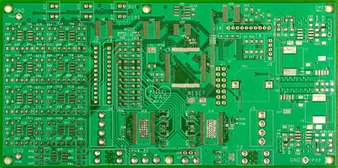
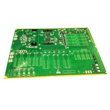
Pcb quality
Importance Of Material Selection In PCB Quality
In the realm of electronics manufacturing, the quality of printed circuit boards (PCBs) is paramount, as it directly influences the performance, reliability, and longevity of electronic devices. A critical factor that significantly impacts PCB quality is the selection of materials. The choice of materials not only affects the electrical properties and thermal management of the PCB but also determines its mechanical strength and durability. Therefore, understanding the importance of material selection is essential for manufacturers aiming to produce high-quality PCBs.
To begin with, the substrate material forms the foundation of a PCB and plays a crucial role in its overall performance.
The most commonly used substrate is FR-4, a composite material made of woven fiberglass cloth with an epoxy resin binder. FR-4 is favored for its excellent balance of cost, mechanical strength, and electrical insulation properties. However, for applications requiring higher performance, such as in high-frequency or high-temperature environments, alternative materials like polyimide, PTFE, or ceramic substrates may be more appropriate. These materials offer superior thermal stability and dielectric properties, albeit at a higher cost, thus underscoring the need for careful consideration based on the specific application requirements.
Moreover, the choice of copper cladding is another vital aspect of material selection that affects PCB quality.
Copper is used for the conductive traces on a PCB, and its thickness can vary depending on the current-carrying requirements of the circuit. Thicker copper layers are necessary for high-power applications to ensure efficient current flow and minimize resistive losses. However, thicker copper can also increase the cost and complexity of the manufacturing process. Therefore, selecting the appropriate copper thickness is a balancing act between performance needs and cost constraints.
In addition to substrate and copper materials, the selection of solder mask and surface finish also plays a significant role in determining PCB quality.
The solder mask, typically a polymer layer applied over the copper traces, protects against oxidation and prevents solder bridges during assembly. The choice of solder mask material can affect the PCB’s thermal and chemical resistance, impacting its reliability in harsh environments. Similarly, the surface finish, which provides a protective coating over the exposed copper pads, is crucial for ensuring good solderability and preventing corrosion. Common finishes include HASL (Hot Air Solder Leveling), ENIG (Electroless Nickel Immersion Gold), and OSP (Organic Solderability Preservative), each offering distinct advantages and trade-offs in terms of cost, durability, and ease of assembly.
Furthermore, the environmental impact of material selection cannot be overlooked.
With increasing emphasis on sustainability, manufacturers are encouraged to choose materials that are environmentally friendly and comply with regulations such as RoHS (Restriction of Hazardous Substances). This consideration not only enhances the PCB’s marketability but also aligns with global efforts to reduce electronic waste and promote eco-friendly manufacturing practices.
In conclusion, the importance of material selection in PCB quality cannot be overstated. It requires a comprehensive understanding of the electrical, thermal, mechanical, and environmental demands of the intended application. By carefully selecting the appropriate materials, manufacturers can ensure that their PCBs meet the desired performance standards while also addressing cost and sustainability concerns. As technology continues to advance, the need for high-quality PCBs will only grow, making material selection an ever more critical aspect of the electronics manufacturing process.
Impact Of Manufacturing Processes On PCB Reliability
The reliability of printed circuit boards (PCBs) is a critical factor in the performance and longevity of electronic devices. As the backbone of electronic systems, PCBs must be manufactured with precision and care to ensure they meet the rigorous demands of modern technology. The manufacturing processes involved in PCB production play a pivotal role in determining their quality and reliability. Understanding these processes and their impact on PCB reliability is essential for manufacturers aiming to produce high-quality electronic components.
To begin with, the choice of materials used in PCB manufacturing significantly influences their reliability.
High-quality substrates, such as FR-4, are commonly used due to their excellent thermal and electrical properties. The selection of appropriate materials ensures that the PCB can withstand various environmental stresses, such as temperature fluctuations and humidity, which are common in many applications. Furthermore, the use of high-quality copper for the conductive layers is crucial, as it affects the board’s electrical performance and durability. Poor material choices can lead to issues such as delamination, warping, and electrical failures, which compromise the PCB’s reliability.
In addition to material selection, the precision of the manufacturing processes is equally important.
The etching process, for instance, must be meticulously controlled to ensure that the copper traces are accurately formed. Any deviations in this process can result in short circuits or open circuits, which can severely impact the functionality of the PCB. Similarly, the drilling process, which creates the vias and holes necessary for component placement and interlayer connections, must be executed with high precision. Misaligned or improperly sized holes can lead to poor electrical connections and mechanical instability.
Moreover, the soldering process, which attaches components to the PCB, is a critical step that affects reliability.
The use of high-quality solder and precise temperature control during reflow soldering are essential to prevent defects such as cold joints, solder bridges, and voids. These defects can lead to intermittent connections or complete failure of the PCB. Additionally, the implementation of surface finish techniques, such as HASL (Hot Air Solder Leveling) or ENIG (Electroless Nickel Immersion Gold), provides a protective layer that enhances solderability and prevents oxidation, further contributing to the board’s reliability.
Furthermore, the testing and inspection stages of PCB manufacturing are vital in ensuring reliability.
Techniques such as automated optical inspection (AOI) and X-ray inspection are employed to detect defects that may have occurred during production. These inspections help identify issues such as misaligned components, solder defects, and internal structural problems, allowing manufacturers to address them before the PCBs are deployed in electronic devices. Rigorous testing, including electrical testing and thermal cycling, also ensures that the PCBs can perform reliably under various conditions.
In conclusion, the reliability of PCBs is heavily influenced by the manufacturing processes employed.
From material selection to precision in etching, drilling, and soldering, each step plays a crucial role in determining the final quality of the PCB. By adhering to stringent manufacturing standards and employing advanced inspection techniques, manufacturers can produce PCBs that meet the high reliability demands of modern electronic applications. As technology continues to evolve, the importance of reliable PCBs will only grow, making it imperative for manufacturers to continually refine their processes to ensure the highest quality outcomes.

Role Of Quality Control In Ensuring PCB Performance
In the realm of electronics manufacturing, the role of quality control in ensuring printed circuit board (PCB) performance cannot be overstated. As the backbone of virtually all electronic devices, PCBs are integral to the functionality and reliability of the end product. Therefore, maintaining high standards of quality control throughout the PCB manufacturing process is essential to meet the rigorous demands of modern technology.
To begin with, quality control in PCB manufacturing involves a series of systematic procedures designed to detect and rectify defects at various stages of production.
This process starts with the careful selection of raw materials, as the quality of the substrate, copper foil, and other components directly impacts the performance of the final product. By ensuring that only high-grade materials are used, manufacturers can significantly reduce the likelihood of defects that could compromise the PCB’s functionality.
Moreover, the precision of the manufacturing process itself is crucial.
Advanced techniques such as automated optical inspection (AOI) and X-ray inspection are employed to identify any discrepancies in the PCB’s design and structure. These technologies allow for the detection of minute defects that might otherwise go unnoticed, such as misalignments, soldering issues, or micro-cracks. By addressing these issues early in the production process, manufacturers can prevent costly rework and ensure that the final product meets the required specifications.
In addition to these inspection techniques, rigorous testing is a cornerstone of quality control in PCB manufacturing.
Functional testing, for instance, evaluates the PCB’s performance under various conditions to ensure it operates as intended. This step is vital for identifying potential weaknesses that could lead to failure in real-world applications. Furthermore, environmental testing exposes the PCB to extreme temperatures, humidity, and other stressors to assess its durability and reliability over time. By simulating these conditions, manufacturers can gain valuable insights into the PCB’s long-term performance and make necessary adjustments to enhance its resilience.
Transitioning from the technical aspects, it is important to consider the role of quality control in fostering customer trust and satisfaction.
In an industry where precision and reliability are paramount, any lapse in quality can have significant repercussions. Defective PCBs can lead to device malfunctions, costly recalls, and damage to a company’s reputation. Therefore, by implementing robust quality control measures, manufacturers not only safeguard their products but also build confidence among their clients. This trust is crucial for maintaining long-term business relationships and securing a competitive edge in the market.
Furthermore, the emphasis on quality control aligns with the growing demand for sustainable manufacturing practices.
By minimizing defects and waste, manufacturers can reduce their environmental footprint and contribute to a more sustainable future. This approach not only benefits the environment but also enhances the company’s image as a responsible and forward-thinking entity.
In conclusion, the role of quality control in ensuring PCB performance is multifaceted and indispensable. From the selection of materials to the implementation of advanced inspection and testing techniques, every step in the manufacturing process is geared towards achieving the highest standards of quality. By doing so, manufacturers can deliver reliable and durable PCBs that meet the evolving needs of the electronics industry, while also fostering customer trust and promoting sustainable practices. As technology continues to advance, the importance of quality control in PCB manufacturing will only grow, underscoring its critical role in shaping the future of electronics.
Advances In PCB Testing Techniques For Enhanced Quality
Printed Circuit Boards (PCBs) are the backbone of modern electronic devices, serving as the foundation upon which complex circuits are built. As technology advances, the demand for high-quality PCBs has become increasingly critical, necessitating the development of sophisticated testing techniques to ensure their reliability and performance. In recent years, significant strides have been made in PCB testing methodologies, enhancing the quality and dependability of these essential components.
To begin with, one of the most notable advancements in PCB testing is the integration of automated optical inspection (AOI) systems.
These systems utilize high-resolution cameras and advanced algorithms to meticulously examine PCBs for defects such as misaligned components, soldering issues, and surface irregularities. By automating the inspection process, AOI systems significantly reduce the likelihood of human error, thereby improving the overall quality of the PCBs. Moreover, the speed and precision of AOI systems allow for rapid identification and rectification of defects, ensuring that only flawless boards proceed to the next stages of production.
In addition to AOI, X-ray inspection has emerged as a pivotal technique in PCB testing. .
This method is particularly effective for detecting hidden defects that are not visible to the naked eye, such as voids in solder joints or internal layer misalignments. By providing a non-destructive means of examining the internal structure of PCBs, X-ray inspection ensures that even the most minute imperfections are identified and addressed. Consequently, this technique plays a crucial role in enhancing the reliability and longevity of PCBs, especially in applications where failure is not an option.
Furthermore, advancements in in-circuit testing (ICT) have also contributed to improved PCB quality.
ICT involves the use of specialized test fixtures and probes to evaluate the electrical performance of individual components on a PCB. By verifying parameters such as resistance, capacitance, and signal integrity, ICT ensures that each component functions as intended within the circuit. The precision and comprehensiveness of ICT make it an indispensable tool for detecting functional defects early in the production process, thereby preventing costly rework and ensuring that only high-quality boards reach the market.
Another significant development in PCB testing is the adoption of boundary scan technology.
This technique leverages the IEEE 1149.1 standard, commonly known as JTAG, to test the interconnections between integrated circuits on a PCB. By facilitating access to otherwise inaccessible test points, boundary scan technology enables thorough testing of complex boards with high component density. This capability is particularly valuable in the context of modern electronics, where miniaturization and increased functionality are driving the need for more intricate PCB designs.
Moreover, the integration of machine learning and artificial intelligence (AI) into PCB testing processes is poised to revolutionize the industry.
By analyzing vast amounts of test data, AI algorithms can identify patterns and predict potential defects with remarkable accuracy. This predictive capability not only enhances the efficiency of testing processes but also enables proactive quality control measures, ultimately leading to higher-quality PCBs.
In conclusion, the continuous evolution of PCB testing techniques is instrumental in ensuring the production of high-quality boards that meet the rigorous demands of modern electronics. From automated optical inspection and X-ray analysis to in-circuit testing and boundary scan technology, these advancements collectively contribute to the reliability and performance of PCBs. As the industry continues to innovate, the integration of machine learning and AI promises to further elevate PCB quality, paving the way for more robust and dependable electronic devices.