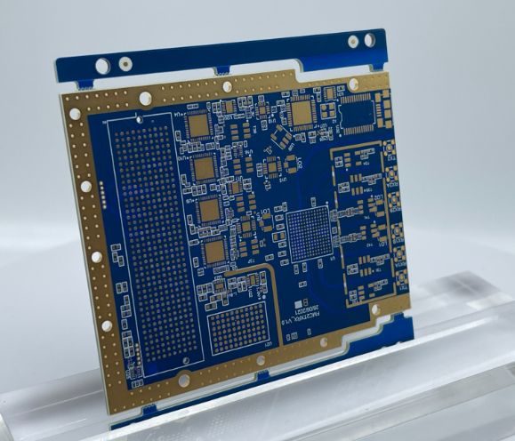
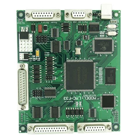
Non hdi pcb
Understanding Non HDI PCB: Key Differences and Applications
In the realm of electronics manufacturing, printed circuit boards (PCBs) serve as the foundational building blocks for a wide array of devices. Among the various types of PCBs, non-high-density interconnect (non-HDI) PCBs are a prevalent choice for many applications. Understanding the key differences between non-HDI and HDI PCBs, as well as their specific applications, is crucial for making informed decisions in electronics design and manufacturing.
Non-HDI PCBs, often referred to as standard PCBs, are characterized by their relatively simple design and construction compared to their HDI counterparts.
These boards typically feature larger trace widths and spacing, fewer layers, and through-hole components. The manufacturing process for non-HDI PCBs is generally less complex, which can result in lower production costs and shorter lead times. This simplicity makes non-HDI PCBs an attractive option for a variety of applications where high-density interconnects are not a critical requirement.
One of the primary differences between non-HDI and HDI PCBs lies in their layer count and interconnect density.
Non-HDI PCBs usually have fewer layers, often ranging from one to four, whereas HDI PCBs can have multiple layers with microvias and blind or buried vias to accommodate higher component density. This distinction is significant because it influences the overall size and weight of the final product. Non-HDI PCBs are typically used in applications where space constraints are not a major concern, allowing for larger and more robust designs.
Moreover, the choice between non-HDI and HDI PCBs can also be influenced by the complexity of the electronic device.
Non-HDI PCBs are well-suited for simpler electronic devices that do not require the intricate routing and miniaturization capabilities of HDI technology. For instance, consumer electronics such as basic household appliances, toys, and simple communication devices often utilize non-HDI PCBs due to their cost-effectiveness and adequate performance for these applications.
In addition to cost and complexity considerations, the thermal management capabilities of non-HDI PCBs can be advantageous in certain scenarios.
The larger trace widths and spacing in non-HDI designs can facilitate better heat dissipation, which is beneficial for applications involving high power or heat generation. This makes non-HDI PCBs a suitable choice for power supplies, industrial equipment, and other applications where thermal management is a priority.
Furthermore, the reliability and ease of repair associated with non-HDI PCBs are noteworthy.
The use of through-hole components and larger traces can simplify the repair process, as components are easier to access and replace. This aspect is particularly valuable in industries where maintenance and longevity are critical, such as automotive and aerospace sectors.
In conclusion, non-HDI PCBs offer a range of benefits that make them a viable option for numerous applications.
Their simpler design, cost-effectiveness, and thermal management capabilities make them suitable for devices where high-density interconnects are not essential. By understanding the key differences between non-HDI and HDI PCBs, manufacturers and designers can make informed decisions that align with the specific requirements of their projects. As technology continues to evolve, the role of non-HDI PCBs remains significant, providing a reliable and efficient solution for a wide array of electronic devices.
Design Challenges and Solutions for Non-HDI PCB
In the realm of printed circuit board (PCB) design, non-high-density interconnect (non-HDI) PCBs continue to play a crucial role in various applications, despite the growing popularity of HDI technology. Non-HDI PCBs, characterized by their traditional design and manufacturing processes, present unique design challenges that require careful consideration and innovative solutions. Understanding these challenges and the strategies to overcome them is essential for engineers and designers aiming to optimize the performance and reliability of non-HDI PCBs.
One of the primary challenges in non-HDI PCB design is managing the board’s size and layer count.
Unlike HDI PCBs, which utilize microvias and finer lines to achieve higher component density, non-HDI PCBs often require more layers to accommodate complex circuits. This can lead to increased board thickness, which may affect the overall form factor and weight of the final product. To address this issue, designers must employ efficient layout strategies, such as optimizing component placement and routing paths, to minimize the number of layers without compromising functionality.
Another significant challenge is signal integrity, which can be compromised by factors such as crosstalk, electromagnetic interference (EMI), and impedance mismatches.
Non-HDI PCBs, with their larger trace widths and spacing, are more susceptible to these issues compared to their HDI counterparts. To mitigate signal integrity problems, designers can implement techniques such as differential signaling, proper grounding, and the use of shielding materials. Additionally, careful attention to trace length matching and controlled impedance routing can help maintain signal quality across the board.
Thermal management is also a critical consideration in non-HDI PCB design.
As electronic components become more powerful, they generate more heat, which can lead to performance degradation or even failure if not properly managed. Non-HDI PCBs, with their thicker layers and larger components, may face challenges in dissipating heat effectively. To overcome this, designers can incorporate thermal vias, heat sinks, and thermal pads to enhance heat dissipation. Moreover, selecting materials with high thermal conductivity and designing for optimal airflow can further improve thermal performance.
Furthermore, manufacturability and cost are important factors in non-HDI PCB design.
The traditional manufacturing processes used for non-HDI PCBs, such as through-hole technology, can be more cost-effective than the advanced techniques required for HDI PCBs. However, designers must still consider the trade-offs between cost and performance. By collaborating closely with manufacturers during the design phase, engineers can ensure that the PCB design is optimized for production, reducing the likelihood of costly revisions and delays.
In addition to these technical challenges, non-HDI PCB designers must also navigate the evolving landscape of industry standards and regulations.
Compliance with standards such as IPC and RoHS is essential to ensure product safety and reliability. Staying informed about the latest developments in these standards and incorporating them into the design process can help designers avoid potential compliance issues.
In conclusion, while non-HDI PCBs may not offer the same level of miniaturization and complexity as HDI PCBs, they remain a vital component of many electronic systems. By addressing the challenges of size, signal integrity, thermal management, manufacturability, and compliance, designers can create non-HDI PCBs that meet the demands of modern applications. Through innovative design strategies and close collaboration with manufacturers, the potential of non-HDI PCBs can be fully realized, ensuring their continued relevance in the ever-evolving field of electronics.

Cost-Effective Manufacturing Techniques for Non-HDI PCB
In the realm of printed circuit board (PCB) manufacturing, the distinction between high-density interconnect (HDI) and non-HDI PCBs is significant, particularly when considering cost-effective manufacturing techniques. Non-HDI PCBs, characterized by their simpler design and lower layer count, offer a range of opportunities for cost savings without compromising on quality or performance. Understanding the nuances of these techniques is essential for manufacturers aiming to optimize production efficiency and reduce expenses.
To begin with, material selection plays a crucial role in the cost-effective manufacturing of non-HDI PCBs.
Unlike HDI PCBs, which often require advanced materials to support their complex structures, non-HDI PCBs can utilize more conventional materials such as FR-4. This widely used substrate is not only cost-effective but also provides adequate thermal and mechanical properties for a variety of applications. By opting for standard materials, manufacturers can significantly reduce material costs while maintaining the necessary performance standards.
Furthermore, the manufacturing process itself offers several avenues for cost reduction.
One of the primary techniques is panelization, which involves arranging multiple PCBs on a single panel during production. This approach maximizes the use of raw materials and minimizes waste, thereby lowering overall production costs. Additionally, panelization can streamline the assembly process, as multiple boards can be processed simultaneously, reducing labor and time expenses.
Another effective technique is the use of automated assembly lines.
Automation in PCB manufacturing not only enhances precision and consistency but also reduces labor costs. By employing automated pick-and-place machines, manufacturers can efficiently place components on non-HDI PCBs with high accuracy, minimizing the risk of errors and rework. This not only speeds up the production process but also ensures a higher yield, further contributing to cost savings.
Moreover, design for manufacturability (DFM) principles are integral to cost-effective non-HDI PCB production.
By designing PCBs with manufacturing constraints in mind, engineers can simplify the production process and reduce the likelihood of costly errors. For instance, minimizing the number of vias and layers can lead to simpler designs that are easier and cheaper to produce. Additionally, standardizing component sizes and placements can facilitate automated assembly, further driving down costs.
In addition to these techniques, efficient supply chain management is vital for cost-effective manufacturing.
Establishing strong relationships with suppliers can lead to better pricing on materials and components, as well as more reliable delivery schedules. By negotiating favorable terms and maintaining a steady flow of materials, manufacturers can avoid production delays and reduce inventory costs.
Finally, continuous improvement and quality control are essential components of cost-effective non-HDI PCB manufacturing.
By implementing rigorous testing and inspection protocols, manufacturers can identify and address defects early in the production process, preventing costly rework and ensuring high-quality outputs. Moreover, adopting lean manufacturing principles can help eliminate waste and optimize processes, further enhancing cost efficiency.
In conclusion, the cost-effective manufacturing of non-HDI PCBs hinges on a combination of strategic material selection, efficient production techniques, and robust supply chain management. By leveraging these approaches, manufacturers can achieve significant cost savings while maintaining the quality and reliability of their products. As the demand for non-HDI PCBs continues to grow across various industries, these techniques will remain crucial for manufacturers seeking to stay competitive in an ever-evolving market.
Material Selection and Performance Considerations in Non-HDI PCB
In the realm of printed circuit boards (PCBs), the selection of materials plays a pivotal role in determining the performance and reliability of the final product. While High-Density Interconnect (HDI) PCBs have gained popularity due to their ability to support complex and compact designs, non-HDI PCBs remain a staple in various applications, particularly where cost-effectiveness and simplicity are prioritized. Understanding the material selection and performance considerations for non-HDI PCBs is essential for engineers and designers aiming to optimize their designs for specific applications.
To begin with, the choice of substrate material is fundamental in non-HDI PCB design.
The most commonly used substrate is FR-4, a composite material made of woven fiberglass cloth with an epoxy resin binder. FR-4 is favored for its excellent mechanical strength, electrical insulation properties, and cost-effectiveness. However, depending on the specific requirements of the application, alternative materials such as polyimide, PTFE, or metal-core substrates may be considered. These materials offer distinct advantages, such as higher thermal stability or improved signal integrity, which can be crucial in certain environments.
Transitioning to the consideration of copper cladding, the thickness of the copper layer is another critical factor influencing the performance of non-HDI PCBs.
Standard copper thicknesses range from 0.5 oz/ft² to 2 oz/ft², with thicker copper layers providing better current-carrying capacity and enhanced thermal management. However, thicker copper can also increase the overall weight and cost of the PCB. Therefore, designers must carefully balance these factors to meet the specific electrical and thermal requirements of their application.
Furthermore, the choice of solder mask material is vital in protecting the PCB from environmental factors and ensuring reliable performance.
Solder masks are typically made from epoxy-based materials, which provide good adhesion and chemical resistance. However, for applications requiring higher thermal resistance or flexibility, alternative materials such as liquid photoimageable (LPI) solder masks or flexible solder masks may be employed. The selection of the appropriate solder mask material can significantly impact the durability and longevity of the PCB, especially in harsh operating conditions.
In addition to material selection, performance considerations such as signal integrity and thermal management are paramount in non-HDI PCB design.
Signal integrity is influenced by factors such as trace width, spacing, and the dielectric properties of the substrate material. Ensuring proper impedance matching and minimizing signal loss are crucial for maintaining the integrity of high-speed signals. On the other hand, thermal management involves the efficient dissipation of heat generated by electronic components. This can be achieved through the use of thermal vias, heat sinks, or the selection of materials with high thermal conductivity.
In conclusion, the material selection and performance considerations in non-HDI PCB design are multifaceted and require a comprehensive understanding of the application’s specific requirements. By carefully selecting the appropriate substrate, copper cladding, and solder mask materials, and by addressing signal integrity and thermal management challenges, designers can optimize the performance and reliability of non-HDI PCBs. As technology continues to evolve, staying informed about advancements in materials and design techniques will be essential for engineers and designers striving to meet the ever-changing demands of the electronics industry.