Multilayer printed circuit board process
Understanding The Basics Of Multilayer PCB Design
In the realm of modern electronics, multilayer printed circuit boards (PCBs) have become indispensable due to their ability to accommodate complex circuitry within a compact form. Understanding the basics of multilayer PCB design is crucial for engineers and designers who aim to optimize the performance and reliability of electronic devices. At its core, a multilayer PCB consists of multiple layers of conductive material, typically copper, separated by insulating layers known as substrates. These layers are laminated together under high pressure and temperature to form a single, cohesive unit. The primary advantage of this configuration is the increased circuit density, which allows for more complex and powerful electronic devices.
To begin with, the design process of a multilayer PCB involves several critical steps, starting with the conceptualization of the circuit.
Designers must first determine the number of layers required, which is influenced by the complexity of the circuit and the space constraints of the final product. Typically, multilayer PCBs can range from four to over twenty layers, with each additional layer providing more routing options and greater functionality. Once the number of layers is decided, the next step involves creating a schematic diagram that outlines the electrical connections and components.
Following the schematic design, the layout process begins, which involves placing components on the board and routing the electrical connections between them.
This stage is crucial as it directly impacts the performance and manufacturability of the PCB. Designers must consider factors such as signal integrity, thermal management, and electromagnetic interference, all of which can affect the functionality of the final product. Advanced software tools are often employed to simulate and optimize the layout, ensuring that the design meets the necessary specifications.
As the design progresses, attention must be paid to the stack-up configuration, which refers to the arrangement of the conductive and insulating layers.
A well-planned stack-up can significantly enhance the electrical performance of the PCB by minimizing signal loss and crosstalk between layers. Additionally, the choice of materials for both the conductive and insulating layers is critical, as it affects the board’s thermal and mechanical properties. Common materials include FR-4 for the substrate and copper for the conductive layers, although other materials may be used depending on the specific requirements of the application.
Once the design is finalized, the manufacturing process begins.
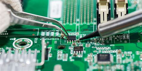
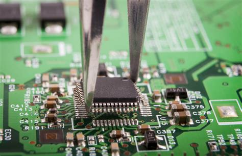
This involves several stages, including the fabrication of individual layers, the alignment and lamination of these layers, and the drilling of vias, which are small holes that allow electrical connections between layers. Each step must be executed with precision to ensure the integrity and functionality of the final product. Quality control measures, such as electrical testing and inspection, are implemented throughout the manufacturing process to identify and rectify any defects.
In conclusion, the design and manufacturing of multilayer PCBs is a complex process that requires careful planning and execution. By understanding the basics of multilayer PCB design, engineers and designers can create high-performance electronic devices that meet the demands of today’s technology-driven world. As electronic devices continue to evolve, the role of multilayer PCBs will undoubtedly remain pivotal, driving innovation and enabling the development of increasingly sophisticated technologies.
Key Steps In The Multilayer PCB Manufacturing Process
The manufacturing process of multilayer printed circuit boards (PCBs) is a complex and intricate procedure that requires precision and attention to detail. This process begins with the design phase, where engineers use specialized software to create a detailed blueprint of the PCB. The design includes the layout of the circuitry, the placement of components, and the routing of electrical connections. Once the design is finalized, it is converted into a format suitable for manufacturing, typically a Gerber file, which serves as a guide for the subsequent steps.
Following the design phase, the next step is the preparation of the raw materials.
This involves selecting high-quality substrates, such as fiberglass-reinforced epoxy resin, which serve as the base material for the PCB. Copper foil is then laminated onto these substrates to form the conductive layers. The number of layers in a multilayer PCB can vary, but typically ranges from four to twelve, depending on the complexity of the circuit.
Once the materials are prepared, the process of creating the individual layers begins.
This involves a series of photolithographic steps, where each layer of the PCB is coated with a photosensitive material. The Gerber files are used to create photomasks, which are then aligned with the coated layers. Ultraviolet light is used to expose the photomask pattern onto the photosensitive material, hardening the exposed areas. The unexposed areas are then removed using a chemical developer, revealing the desired circuit pattern.
After the circuit patterns are established, the next step is etching.
This process involves immersing the layers in a chemical solution that removes the unwanted copper, leaving behind the circuit traces. Once etching is complete, the layers undergo a thorough cleaning process to remove any residual chemicals and debris.
The individual layers are then aligned and laminated together under high pressure and temperature to form a single, cohesive unit.
This step is crucial, as any misalignment can lead to electrical failures or short circuits. The laminated board is then drilled to create holes for component leads and vias, which are used to connect the different layers electrically.
Following drilling, the holes are plated with copper to ensure electrical conductivity between the layers.
This is achieved through an electroplating process, where the board is submerged in a copper sulfate solution and an electric current is applied. The copper ions in the solution are deposited onto the exposed surfaces, forming a conductive layer.
The final steps in the manufacturing process involve applying a solder mask and silkscreen.
The solder mask is a protective layer that prevents solder bridges and short circuits during component assembly. It is typically green, although other colors are available. The silkscreen is used to print labels and markings on the PCB, aiding in component placement and identification.
In conclusion, the manufacturing process of multilayer PCBs is a meticulous and highly technical procedure that requires careful planning and execution. Each step, from design to final assembly, plays a critical role in ensuring the functionality and reliability of the finished product. As technology continues to advance, the demand for more complex and compact PCBs will only increase, driving further innovation in manufacturing techniques and materials.

Challenges And Solutions In Multilayer PCB Fabrication
The fabrication of multilayer printed circuit boards (PCBs) presents a unique set of challenges that require innovative solutions to ensure the reliability and functionality of the final product. As electronic devices become increasingly complex, the demand for multilayer PCBs has surged, necessitating advancements in manufacturing techniques to address the intricacies involved.
One of the primary challenges in multilayer PCB fabrication is the precise alignment of multiple layers.
Each layer must be accurately aligned to ensure that the electrical connections between them are correctly established. Misalignment can lead to short circuits or open circuits, compromising the performance of the device. To overcome this, manufacturers employ advanced optical alignment systems and employ registration techniques that ensure each layer is perfectly positioned before lamination.
Another significant challenge is the management of thermal expansion.
Different materials used in the construction of PCBs, such as copper and various substrates, have distinct coefficients of thermal expansion. During the fabrication process, especially during the lamination and soldering stages, these materials expand and contract at different rates. This can lead to warping or delamination of the layers, which can be detrimental to the board’s integrity. To mitigate this issue, manufacturers carefully select materials with compatible thermal properties and employ controlled heating and cooling processes to minimize stress on the board.
The aspect of via formation also presents a considerable challenge in multilayer PCB fabrication.
Vias are small holes that allow electrical connections between different layers of the board. In multilayer PCBs, these vias must be precisely drilled and plated to ensure reliable connectivity. The miniaturization of electronic components has led to the need for smaller and more densely packed vias, which increases the complexity of the drilling and plating processes. Advanced laser drilling techniques and improved plating methods have been developed to address these challenges, allowing for the creation of microvias that meet the demands of modern electronic designs.
As the number of layers increases, so does the potential for signal interference and crosstalk between adjacent layers.
This can degrade the performance of high-speed circuits and lead to data loss or corruption. To combat this, designers employ techniques such as controlled impedance routing and the use of ground planes to shield sensitive signals. Additionally, simulation tools are used during the design phase to predict and mitigate potential signal integrity issues before the board is fabricated.
Furthermore, the aspect of signal integrity is a critical consideration in multilayer PCB fabrication.
The environmental impact of multilayer PCB fabrication is another area of concern. The process involves the use of various chemicals and materials that can be harmful if not managed properly. Manufacturers are increasingly adopting environmentally friendly practices, such as using lead-free solder and implementing waste reduction strategies. Recycling and proper disposal of hazardous materials are also prioritized to minimize the ecological footprint of PCB production.
In conclusion, while the fabrication of multilayer PCBs presents numerous challenges, ongoing advancements in technology and manufacturing processes continue to provide effective solutions. Through precise alignment techniques, careful material selection, advanced via formation methods, and attention to signal integrity, manufacturers are able to produce reliable and high-performance multilayer PCBs. As the demand for more complex electronic devices grows, the industry will undoubtedly continue to innovate, ensuring that these challenges are met with increasingly sophisticated solutions.
Innovations In Multilayer PCB Technology And Applications
The evolution of multilayer printed circuit boards (PCBs) has been a cornerstone in the advancement of modern electronics, enabling the development of increasingly complex and compact devices. As technology continues to progress, innovations in multilayer PCB technology have become pivotal in meeting the demands of various industries, from consumer electronics to aerospace. These advancements not only enhance the functionality and reliability of electronic devices but also open new avenues for applications that were previously unattainable.
To begin with, the multilayer PCB process involves the integration of multiple layers of conductive material, typically copper, separated by insulating layers, known as substrates.
This configuration allows for a higher density of components and interconnections, which is essential for the miniaturization of electronic devices. Recent innovations in this process have focused on improving the materials and techniques used in manufacturing, thereby enhancing the performance and durability of the PCBs. For instance, the development of high-frequency laminates has been instrumental in supporting the growing demand for faster data transmission rates, particularly in telecommunications and data processing applications.
Moreover, advancements in fabrication techniques, such as laser drilling and advanced plating methods, have significantly improved the precision and efficiency of multilayer PCB production.
These techniques allow for the creation of smaller vias and finer traces, which are crucial for accommodating the increasing complexity of modern electronic circuits. Additionally, the adoption of automated optical inspection (AOI) systems has enhanced quality control, ensuring that each layer of the PCB is accurately aligned and free of defects. This level of precision is particularly important in applications where reliability is critical, such as in medical devices and automotive systems.
In parallel with these manufacturing innovations, the design of multilayer PCBs has also seen significant progress.
The use of advanced computer-aided design (CAD) software enables engineers to simulate and optimize the performance of PCBs before they are physically produced. This not only reduces the time and cost associated with prototyping but also allows for the exploration of more complex designs that can meet the specific needs of different applications. Furthermore, the integration of embedded components within the PCB layers is becoming increasingly common, offering additional space savings and performance benefits.
The applications of multilayer PCBs are as diverse as they are critical.
In the realm of consumer electronics, they are the backbone of smartphones, tablets, and laptops, where space is at a premium, and performance demands are high. In the automotive industry, multilayer PCBs are essential for the operation of advanced driver-assistance systems (ADAS) and electric vehicle powertrains, where reliability and efficiency are paramount. Additionally, in the aerospace sector, these PCBs are used in avionics and satellite systems, where they must withstand extreme conditions while maintaining optimal performance.
In conclusion, the innovations in multilayer PCB technology are driving significant advancements across various industries, enabling the development of more sophisticated and reliable electronic devices. As the demand for smaller, faster, and more efficient electronics continues to grow, the role of multilayer PCBs will undoubtedly become even more critical. By continually improving materials, manufacturing techniques, and design processes, the industry is well-positioned to meet the challenges of the future, paving the way for new applications and technological breakthroughs.