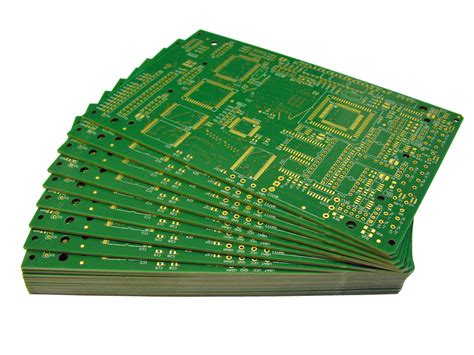
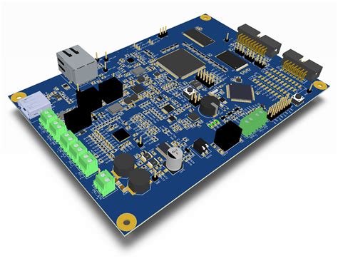
Multilayer ceramic pcb
Advantages Of Multilayer Ceramic PCBs In Modern Electronics
Multilayer ceramic printed circuit boards (PCBs) have emerged as a pivotal component in the realm of modern electronics, offering a multitude of advantages that cater to the ever-evolving demands of technology. As electronic devices become increasingly complex and compact, the need for efficient, reliable, and high-performance circuit boards has never been more critical. Multilayer ceramic PCBs, with their unique properties, address these needs effectively, making them an indispensable choice for a wide range of applications.
One of the primary advantages of multilayer ceramic PCBs is their exceptional thermal conductivity.
Unlike traditional PCBs, which often struggle with heat dissipation, ceramic materials inherently possess superior thermal management capabilities. This characteristic is particularly beneficial in high-power applications where excessive heat can lead to performance degradation or even failure. By efficiently dissipating heat, multilayer ceramic PCBs ensure the longevity and reliability of electronic components, thereby enhancing the overall performance of the device.
In addition to thermal management, multilayer ceramic PCBs offer remarkable electrical insulation properties.
The ceramic material acts as an excellent insulator, preventing electrical interference and ensuring signal integrity. This is crucial in high-frequency applications where signal loss or distortion can significantly impact performance. The ability to maintain signal clarity and reduce electromagnetic interference makes multilayer ceramic PCBs ideal for use in telecommunications, aerospace, and other industries where precision and reliability are paramount.
Furthermore, the compact nature of multilayer ceramic PCBs is another significant advantage.
As electronic devices continue to shrink in size, the demand for smaller, more efficient components has increased. Multilayer ceramic PCBs can accommodate multiple layers of circuitry within a single board, allowing for greater functionality without increasing the overall size of the device. This compactness not only saves space but also reduces the weight of the device, which is particularly advantageous in portable electronics and aerospace applications where weight is a critical factor.
Moreover, the mechanical strength and durability of multilayer ceramic PCBs cannot be overlooked.
Ceramic materials are inherently robust and resistant to environmental factors such as moisture, chemicals, and temperature fluctuations. This resilience ensures that multilayer ceramic PCBs can withstand harsh operating conditions, making them suitable for use in demanding environments such as automotive and industrial applications. The ability to maintain structural integrity under stress further contributes to the reliability and longevity of electronic devices.
In addition to these technical advantages, multilayer ceramic PCBs also offer economic benefits.
While the initial cost of ceramic materials may be higher than that of traditional materials, the long-term savings in terms of reduced maintenance, increased reliability, and extended lifespan often outweigh the initial investment. This cost-effectiveness, combined with the superior performance characteristics, makes multilayer ceramic PCBs an attractive option for manufacturers seeking to optimize their products.
In conclusion, the advantages of multilayer ceramic PCBs in modern electronics are manifold. Their superior thermal management, electrical insulation, compactness, mechanical strength, and economic benefits make them a preferred choice for a wide range of applications. As technology continues to advance, the demand for high-performance, reliable, and efficient circuit boards will only grow, solidifying the role of multilayer ceramic PCBs as a cornerstone of modern electronic design.
Manufacturing Process Of Multilayer Ceramic PCBs
The manufacturing process of multilayer ceramic printed circuit boards (PCBs) is a sophisticated and intricate procedure that demands precision and expertise. These PCBs are integral to various high-performance applications, particularly in industries such as aerospace, telecommunications, and medical devices, where reliability and efficiency are paramount. The process begins with the selection of suitable ceramic materials, which are chosen for their excellent thermal conductivity, electrical insulation properties, and ability to withstand high temperatures. Commonly used ceramics include alumina, aluminum nitride, and beryllium oxide, each offering distinct advantages depending on the specific requirements of the application.
Once the appropriate ceramic material is selected, the next step involves the preparation of ceramic substrates.
This is achieved through a process known as tape casting, where a slurry of ceramic powder, binders, and solvents is spread into thin layers, or tapes, on a flat surface. These tapes are then dried to remove the solvents, resulting in flexible sheets of ceramic material. The thickness of these sheets can be precisely controlled, which is crucial for the subsequent layering process.
Following the preparation of ceramic tapes, the next phase involves the creation of the circuit patterns.
This is typically accomplished through screen printing, a technique that allows for the precise deposition of conductive pastes onto the ceramic tapes. These pastes are usually composed of metal particles, such as silver or gold, suspended in a binder. The screen printing process ensures that the conductive paths are accurately defined, which is essential for the functionality of the final PCB.
After the circuit patterns are established, the individual layers of ceramic tapes are carefully aligned and stacked to form a multilayer structure.
This stacking process is critical, as it determines the electrical connectivity between the different layers. To ensure proper alignment, registration holes are often used, allowing for precise positioning of each layer. Once the layers are stacked, they are laminated together under heat and pressure, which causes the binders in the ceramic tapes to soften and bond the layers into a single, cohesive unit.
The laminated stack is then subjected to a sintering process, where it is heated to a high temperature in a controlled atmosphere.
This step is crucial as it facilitates the densification of the ceramic material, enhancing its mechanical strength and electrical properties. During sintering, the metal particles in the conductive pastes also coalesce to form solid conductive paths, ensuring reliable electrical connections throughout the multilayer structure.
Following sintering, the multilayer ceramic PCB undergoes a series of finishing processes.
These may include the application of protective coatings, the addition of surface mount components, and the attachment of connectors. Each of these steps is meticulously executed to ensure the final product meets the stringent quality standards required for its intended application.
In conclusion, the manufacturing process of multilayer ceramic PCBs is a complex and highly specialized endeavor that combines advanced materials science with precision engineering. From the initial selection of ceramic materials to the final assembly and testing, each step is carefully controlled to produce PCBs that offer superior performance and reliability. As technology continues to advance, the demand for these high-performance PCBs is expected to grow, driving further innovations in their manufacturing processes.
Applications Of Multilayer Ceramic PCBs In High-Frequency Devices
Multilayer ceramic printed circuit boards (PCBs) have emerged as a pivotal technology in the realm of high-frequency devices, offering a range of benefits that make them indispensable in various applications. As the demand for high-performance electronic devices continues to grow, the need for PCBs that can support high-frequency operations without compromising on reliability or efficiency becomes increasingly critical. Multilayer ceramic PCBs, with their unique properties, are well-suited to meet these demands, making them a preferred choice in several high-frequency applications.
One of the primary applications of multilayer ceramic PCBs is in the telecommunications industry, where they are used in devices that require high-speed data transmission.
The ability of these PCBs to handle high frequencies with minimal signal loss is crucial in ensuring the efficient operation of communication devices such as smartphones, satellite systems, and radar equipment. The low dielectric constant and high thermal conductivity of ceramic materials contribute to the superior performance of these PCBs in high-frequency environments, allowing for faster signal propagation and reduced heat generation.
In addition to telecommunications, multilayer ceramic PCBs are extensively used in the aerospace and defense sectors.
These industries demand components that can withstand extreme conditions while maintaining high performance. The inherent robustness and reliability of ceramic materials make multilayer ceramic PCBs ideal for use in military radar systems, avionics, and other critical applications. Their ability to operate effectively in harsh environments, such as high temperatures and radiation-prone areas, ensures that they meet the stringent requirements of aerospace and defense applications.
Moreover, the medical field has also benefited from the integration of multilayer ceramic PCBs in high-frequency devices.
Medical imaging equipment, such as MRI and CT scanners, relies on high-frequency signals to produce accurate images. The precision and stability offered by multilayer ceramic PCBs enhance the performance of these devices, leading to improved diagnostic capabilities. Furthermore, the biocompatibility of ceramic materials makes them suitable for use in implantable medical devices, where they can support high-frequency operations without causing adverse reactions in the human body.
Transitioning to the consumer electronics sector, multilayer ceramic PCBs are increasingly being utilized in high-frequency applications such as wireless charging systems and advanced audio equipment. The miniaturization of electronic components has necessitated the development of PCBs that can accommodate complex circuitry within a compact form factor. Multilayer ceramic PCBs, with their ability to integrate multiple layers of circuitry, provide an effective solution for achieving this miniaturization while maintaining high-frequency performance.
In conclusion, the applications of multilayer ceramic PCBs in high-frequency devices are vast and varied, spanning industries such as telecommunications, aerospace, defense, medical, and consumer electronics. Their unique properties, including high thermal conductivity, low dielectric constant, and robustness, make them an ideal choice for supporting high-frequency operations in demanding environments. As technology continues to advance, the role of multilayer ceramic PCBs in high-frequency applications is expected to grow, driving further innovation and development in this critical area of electronics.
Comparing Multilayer Ceramic PCBs To Traditional PCB Materials
Multilayer ceramic printed circuit boards (PCBs) have emerged as a significant advancement in the field of electronics, offering distinct advantages over traditional PCB materials. As the demand for more compact, efficient, and reliable electronic devices continues to grow, the choice of PCB material becomes increasingly critical. Traditional PCBs, typically made from materials such as FR-4, a composite of woven fiberglass cloth with an epoxy resin binder, have been the industry standard for many years. However, the introduction of multilayer ceramic PCBs presents a compelling alternative, particularly for applications requiring high performance and reliability.
One of the primary advantages of multilayer ceramic PCBs is their superior thermal conductivity.
Ceramic materials inherently possess excellent heat dissipation properties, which are crucial for high-power applications. In contrast, traditional FR-4 materials have relatively poor thermal conductivity, which can lead to overheating and potential failure in high-power or high-frequency applications. This makes multilayer ceramic PCBs particularly suitable for use in environments where thermal management is a critical concern, such as in aerospace, automotive, and telecommunications industries.
Moreover, multilayer ceramic PCBs offer enhanced electrical performance.
The dielectric properties of ceramic materials allow for lower signal loss and higher frequency operation compared to traditional materials. This is particularly beneficial in applications involving microwave and RF circuits, where signal integrity is paramount. The ability to maintain signal integrity at high frequencies makes multilayer ceramic PCBs an attractive option for advanced communication systems and radar technologies.
In addition to thermal and electrical advantages, multilayer ceramic PCBs also exhibit superior mechanical properties.
They are more robust and resistant to environmental stressors such as moisture, chemicals, and temperature fluctuations. This durability ensures a longer lifespan and greater reliability, which are essential attributes for mission-critical applications. Traditional PCBs, while generally reliable, can suffer from delamination and other mechanical failures under extreme conditions, limiting their use in certain high-stress environments.
Furthermore, the miniaturization potential of multilayer ceramic PCBs cannot be overlooked.
As electronic devices continue to shrink in size, the ability to pack more functionality into a smaller footprint becomes increasingly important. Multilayer ceramic PCBs allow for higher component density and more complex circuit designs without compromising performance. This is achieved through the use of advanced manufacturing techniques that enable the integration of multiple layers of circuitry within a single ceramic substrate.
Despite these advantages, it is important to acknowledge that multilayer ceramic PCBs are not without their challenges.
The cost of production is generally higher than that of traditional PCBs, primarily due to the complexity of the manufacturing process and the cost of raw materials. Additionally, the design and fabrication of multilayer ceramic PCBs require specialized expertise and equipment, which may not be readily available in all manufacturing facilities.
In conclusion, while traditional PCB materials like FR-4 continue to serve a wide range of applications effectively, multilayer ceramic PCBs offer distinct benefits that make them an attractive choice for specific high-performance and high-reliability applications. Their superior thermal, electrical, and mechanical properties, coupled with their potential for miniaturization, position them as a valuable alternative in the ever-evolving landscape of electronic design and manufacturing. As technology continues to advance, the role of multilayer ceramic PCBs is likely to expand, offering new possibilities for innovation in the electronics industry.