Mastering Double Layer PCB Manufacturing for Enhanced Performance
Key Takeaways
Mastering double layer PCB manufacturing is essential for anyone looking to excel in the world of electronics. As you dive into this technology, it’s important to recognize that the key processes involved play a pivotal role in achieving high-quality results. The choice of materials also significantly impacts the overall PCB manufacturing cost; opting for quality components can enhance durability and performance. Many PCB manufacturing companies are now adopting advanced techniques to improve the efficiency of their processes, leading to superior products that stand out in a competitive market. Understanding the intricacies of your design ensures that you leverage the advantages provided by double layer designs, which can facilitate better signal integrity and reduce electromagnetic interference. As you further explore the nuances of this field, you will find that balancing cost-effectiveness with performance remains a major focus for anyone operating within the PCB manufacturing business. Ultimately, grasping these key takeaways allows you to make informed decisions and positions you well for successful outcomes in your projects.
Mastering Double Layer PCB Manufacturing: An Overview
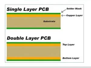
In the realm of PCB manufacturing, double layer boards hold a unique significance, combining functionality with efficiency. You may find that double layer PCBs provide essential advantages over single-layer designs, particularly in terms of space optimization and circuit performance. By utilizing both sides of the substrate, PCB manufacturing companies can significantly reduce the size of the overall design while enhancing signal integrity and reducing electromagnetic interference.
It’s important to recognize that the PCB manufacturing cost for double layer designs can vary based on several factors such as materials chosen, complexity of circuits, and required tolerances. Although initial costs may seem higher than those for simple single-layer boards, the long-term advantages usually outweigh these expenses by improving reliability and reducing repair rates.
The processes involved in creating double layer PCBs are intricate and require attention to detail. Proper design considerations and meticulous assembly techniques directly influence the performance of these boards. For those contemplating entering the PCB manufacturing business, understanding these variables is crucial to ensure you deliver quality products that meet industry standards.
“Investing time in mastering double layer PCB technology is not just beneficial but essential for sustained success in a competitive market.”
| Factor | Impact on Cost |
|---|---|
| Material Quality | Higher costs |
| Design Complexity | Increased pricing |
| Production Volume | Cost efficiencies |
By familiarizing yourself with each aspect of double layer PCB manufacturing, you lay a strong foundation for not only creating superior products but also positioning your business for growth in an ever-evolving technology landscape.
Key Processes in Double Layer PCB Manufacturing
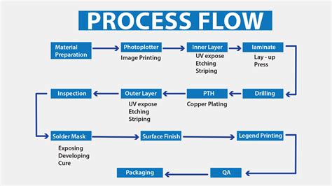
When delving into double layer PCB manufacturing, you will uncover various key processes that contribute to the effectiveness and reliability of your end products. Initially, it involves the assessment of design specifications where you translate your electronic schematic into a workable layout. Designing this layout often utilizes advanced software tools, allowing for precise routing and minimized signal interference, which is integral for performance enhancement in PCB manufacturing.
Subsequently, the lamination process plays a pivotal role; layers of copper and dielectric materials are bonded together under heat and pressure to form the core structure. You might find that choosing high-quality materials can significantly affect the PCB manufacturing cost, impacting overall quality and performance.
Following lamination, the etching stage is crucial in creating the desired electrical pathways. Utilizing chemical etching techniques—often carried out by specialized PCB manufacturing companies—ensures that your circuits are accurately shaped according to specifications. After etching, drilling processes are executed with precision to prepare for component mounting.
Additionally, it’s vital that you consider implementing techniques such as surface finishing options—e.g., HASL or ENIG—which enhance connectivity and surface integrity. Throughout each of these phases in the PCB manufacturing business, maintaining strict quality control is essential. Regular inspections not only validate adherence to standards but also enhance the dependability of your double-layer designs, paving the way for superior electronic applications. Understanding these steps is invaluable as they ultimately determine the functionality and efficacy of your final product.
Materials Used in Double Layer PCB Production
In the realm of pcb manufacturing, the choice of materials is pivotal to achieving optimal performance in double layer PCBs. Typically, you will encounter materials such as FR-4, which is a flame-resistant fiberglass laminate known for its electrical insulating properties. Additionally, Polyimide is favored for applications requiring a higher temperature resistance. Each layer of the PCB is crucial, and the conductive pathways are often comprised of copper, which provides the necessary conductivity and reliability. Furthermore, when you consider the pcb manufacturing cost, it’s essential to factor in the quality and compatibility of these materials, as they directly influence both functionality and durability. Collaborating with reputable pcb manufacturing companies ensures access to high-grade materials that align with industry standards. The overall goal in selecting materials is to enhance the electrical performance while maintaining efficiency in your pcb manufacturing business operations. Understanding these material choices will significantly empower you to design PCBs that meet specific operational requirements without compromising quality. For a deeper dive into material specifications and procurement options, visit Andwin PCB.
Techniques to Enhance Double Layer PCB Performance
Enhancing the performance of double layer PCBs is crucial, especially in today’s rapidly advancing electronic landscape. One effective technique involves optimizing the layout design, which can significantly reduce signal loss and electromagnetic interference. By strategically placing components and using controlled impedance, you can improve signal integrity and overall functionality. Additionally, selecting the appropriate materials is vital; using high-frequency substrates can lead to better performance, minimizing pcb manufacturing costs while ensuring durability. It’s also essential to adjust the via sizes and placement: smaller vias reduce signal paths, thus boosting efficiency. Moreover, implementing techniques such as blind and buried vias can save space, allowing you to create more compact designs without compromising on quality. These enhancements are not just about technical specifications; they are a fundamental aspect of running a successful pcb manufacturing business, especially as you aim to meet growing market demands and compete against other pcb manufacturing companies. By focusing on these techniques, you can elevate your designs to new heights while ensuring a cost-effective production process.
Design Considerations for Double Layer PCBs
When engaging in double layer PCB manufacturing, several critical design considerations must come into play to optimize the performance and functionality of the circuit board. First and foremost, you should evaluate the pcb manufacturing cost associated with your design choices. Incorporating more complex features may require higher costs but can lead to enhanced performance. Space management is vital; ensuring your layout efficiently utilizes both layers can greatly influence signal integrity and power distribution. It’s essential to consider the thermal aspects as well—strategically placing components can help manage heat dissipation effectively. Additionally, selecting suitable materials is crucial; you should collaborate with reputable pcb manufacturing companies that offer high-quality substrates to prevent issues such as warping and reduce electromagnetic interference (EMI). Furthermore, adhering to industry standards and utilizing design rules specific to double layer layouts will ensure that you mitigate potential production challenges. By thoughtfully integrating these considerations, you position your pcb manufacturing business for success in delivering superior electronic applications that harness the full benefits of double layer designs.
Advantages of Double Layer Designs in Electronic Applications
Double layer PCBs offer a myriad of advantages that enhance the performance of electronic applications. One significant benefit is the reduction in pcb manufacturing cost, as these designs allow for more components to be fitted into a smaller space compared to single-layer alternatives. This compactness leads to less material waste and increased efficiency, valuable for your pcb manufacturing business. Moreover, the incorporation of double layers enhances circuit integrity by minimizing signal interference and optimizing routing paths, creating a more reliable product for your customers. When you consider the offerings from various pcb manufacturing companies, you’ll find that double layer designs often come equipped with superior thermal management capabilities, making them ideal for high-performance applications where overheating could be a concern. Additionally, these designs permit greater design flexibility without jeopardizing performance, thus enabling you to innovate effectively while keeping up with the demands of advancing technology. The ability to combine both surface mount and through-hole components further exemplifies why double layer PCBs are essential in modern electronic applications—offering you solutions that are not only efficient but also capable of meeting rigorous industry standards.
Common Challenges in Double Layer PCB Manufacturing
In the realm of pcb manufacturing, you will encounter a variety of challenges that can impact the overall efficacy and reliability of your double layer PCBs. One significant hurdle is achieving precise alignment during the layer stacking process; misalignment can lead to short circuits or signal integrity issues that compromise performance. Additionally, pcb manufacturing companies often face difficulties in maintaining consistent quality across different batches. This inconsistency can stem from variations in materials or equipment calibration, which may increase the overall pcb manufacturing cost if corrective measures are needed.
Moreover, thermal management becomes critical when designing double layer boards. The heat generated during operation must be efficiently dissipated to prevent damage to sensitive components and to ensure optimal functionality. You must also consider the complexities that arise from intricate designs; these may necessitate advanced fabrication techniques that not all pcb manufacturing businesses can readily provide.
Lastly, regulatory compliance poses another layer of complexity in double layer pcb manufacturing. Meeting industry standards for safety and performance requires a comprehensive understanding of not only the materials used but also the processes involved. By being aware of these challenges, you can better strategize your approach towards achieving high-quality double layer PCBs while remaining mindful of production costs and guidance from industry leaders.
Future Trends in Double Layer PCB Technologies
As the demand for advanced electronic devices continues to grow, the landscape of double layer PCB manufacturing is evolving rapidly. One of the most noteworthy trends is the incorporation of high-frequency materials, which significantly enhance the performance of double layer PCBs. This not only optimizes signal integrity but also reduces electromagnetic interference, making it a key focus for PCB manufacturing companies looking to stay competitive.
Another trend reshaping the PCB manufacturing business is the integration of smart technologies, such as automation and artificial intelligence, into production processes. These innovations streamline operations, decrease overall pcb manufacturing cost, and improve design accuracy. Furthermore, advancements in simulation software allow designers to predict potential issues before production begins, ensuring that designs perform flawlessly.
Additionally, sustainability is becoming increasingly prominent in double layer PCB technologies. You can expect more companies to adopt eco-friendly materials and processes as they aim to reduce their environmental footprint. This shift not only appeals to environmentally conscious consumers but also aligns with global regulatory standards.
Incorporating these trends can facilitate a transformative approach to double layer PCB manufacturing, positioning your products for enhanced performance and market success. By staying informed about these developments, you can strategically navigate this dynamic field.
Conclusion
In summary, mastering double layer PCB manufacturing is crucial for achieving enhanced performance in your electronic applications. By understanding the key processes involved and selecting the right materials, you can significantly influence the overall quality of your designs. When you engage with PCB manufacturing companies, consider how they approach PCB manufacturing cost and what techniques they use to elevate performance. Opting for double layer designs not only maximizes space utilization but also increases reliability, making them a preferred choice for many industries. However, it’s essential to be aware of common challenges associated with this manufacturing type and strategize accordingly to overcome them. As technologies evolve, future trends in this sector point toward further innovations that could redefine what’s possible in your PCB manufacturing business. Stay informed and adaptable to ensure you leverage these advancements for optimum outcomes in your projects.

FAQs
What is double layer PCB manufacturing?
Double layer PCB manufacturing refers to the process of creating printed circuit boards that feature two conductive layers, allowing for more complex designs compared to single-layer options.
What are the key advantages of double layer PCBs?
Double layer designs offer increased component density, enhanced electrical performance, and reduced size, making them ideal for various electronic applications. These benefits often contribute to lower pcb manufacturing costs over time.
How do I choose a reliable PCB manufacturing company?
Look for pcb manufacturing companies that have a track record of quality and timely delivery. Consider their expertise in double layer designs specifically, as well as customer reviews and certifications.
What are common challenges faced in double layer PCB manufacturing?
Some challenges include ensuring proper alignment during fabrication, managing thermal expansion, and minimizing the risk of signal interference between layers. It’s vital to address these issues early in your pcb manufacturing business process.
How can I enhance the performance of double layer PCBs?
Utilizing high-quality materials and employing advanced design techniques such as impedance control can significantly improve the performance of your double layer designs.
For more detailed information about pcb manufacturing, please click here.