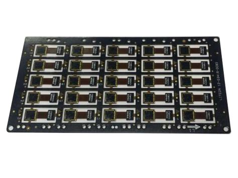
Essential Guide to 6 Layer PCB Fabrication Techniques
Key Takeaways
When embarking on 6 layer PCB fabrication, it’s crucial to understand that mastering the basics can significantly impact your project’s success. For instance, the stack-up design is a foundational element in achieving optimal performance. This involves strategically layering your materials to ensure that signal integrity is maintained throughout the circuit. You should also familiarize yourself with the pcb manufacturing process, which includes various steps from design to production, enabling you to communicate effectively with pcb manufacturing companies.
Moreover, efficient design practices can drastically reduce pcb manufacturing costs. By integrating cost-effective materials, you can strike a balance between performance and budgetary requirements in your pcb manufacturing business. Always keep in mind that addressing common challenges proactively will not only streamline the production process but also enhance overall efficiency. As you navigate these considerations, always remain adaptable and ready to incorporate emerging trends and technologies that can elevate your PCB projects into more advanced territories.
Essential Techniques for 6 Layer PCB Stack-Up Design
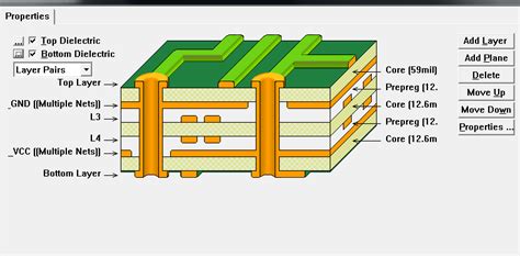
When designing a 6 layer PCB, it’s crucial to understand how the stack-up configuration impacts signal integrity, thermal management, and overall performance. You should start by organizing your layers effectively, often combining signal, power, and ground layers to minimize noise and enhance performance. A common recommendation is to place your power and ground layers adjacent to the signal layers; this not only improves electromagnetic compatibility but also provides better impedance control.
Example Stack-Up Configuration
| Layer Number | Layer Type | Purpose |
|---|---|---|
| 1 | Signal | Primary signal layer |
| 2 | Ground | Ground reference layer |
| 3 | Power | Provides power distribution |
| 4 | Signal | Secondary signal layer |
| 5 | Power/Ground | Additional power or split ground |
| 6 | Signal | Final signal layer |
You should also consider the pcb manufacturing processes that support your stack-up choices. This includes evaluating various pcb manufacturing companies that can handle complex designs. Take note of different fabricators’ capabilities when it comes to handling specific materials, as not all manufacturers are equipped for advanced multilayer designs. The aim is to optimize the pcb manufacturing cost while ensuring high-quality production that meets your requirements.
Additionally, be mindful of aspects like layer thickness, which can significantly impact both performance and costs. Properly planning your stack-up can lead to reduced waste during production, ultimately contributing positively to your pcb manufacturing business model. By employing these techniques and understanding their implications in the real world, you can set a solid foundation for an efficient and successful PCB design process.
Understanding the 6 Layer PCB Manufacturing Process
When diving into 6 layer PCB fabrication, it’s crucial to comprehend the intricate pcb manufacturing process involved. A standard approach begins with the design phase, where you must ensure your schematic and layout are optimized for multilayer configurations. Following this, you’ll transition into preliminary steps such as layer stack-up design, which lays the foundation for your pcb manufacturing project. As you engage with various pcb manufacturing companies, ensure that they employ high-quality materials and technology, as this significantly affects the overall quality and durability of the final product.
During this stage, it’s also important to keep a close eye on pcb manufacturing costs. These can fluctuate based on material choices, layer count, and even the specific processes used by different manufacturers. Understanding these factors can enable you to budget effectively while still achieving high-quality results.
In addition to design considerations, you’ll need to familiarize yourself with different production methods that these pcb manufacturing companies utilize. Techniques such as controlled impedance routing and surface mount technology are essential for ensuring that your 6 layer PCB performs optimally under various conditions. By grasping these details, you’ll increase not only your efficiency in working with a pcb manufacturing business, but also enhance the reliability of your end product. It’s essential to stress that mastering this process will significantly contribute to both performance and cost-effectiveness in your projects.
Practical Tips for Efficient 6 Layer PCB Design
Designing a 6 layer PCB requires a keen understanding of various factors that can enhance your efficiency and output quality. To begin with, ensure your pcb manufacturing process is well-planned, focusing on the stack-up configuration. A well-thought-out stack-up can significantly affect the thermal and electrical performance of your PCB. When you select pcb manufacturing companies, evaluate their experience with multi-layer designs; this experience can often lead to better outcomes.
Additionally, consider the pcb manufacturing cost at every stage of your design. Take advantage of software tools that allow you to simulate various designs before finalization; this will help you identify potential issues earlier in the process. Always remember to prioritize layer-to-layer connectivity, as it is critical in achieving a reliable end-product.
Furthermore, be proactive about selecting appropriate materials suited for high-frequency applications when needed. Using high-quality materials will enhance signal integrity and minimize losses. As you go through your design and fabrication journey, keep an open line of communication with your manufacturer to discuss any concerns or suggestions that arise.
“Investing time upfront in thorough planning can save significant costs and time during the pcb manufacturing business process.”
By adhering to these practical tips, you will streamline your efforts in creating efficient 6 layer PCBs, ultimately leading to more successful projects.
Common Challenges in 6 Layer PCB Fabrication and Solutions
When engaging in 6 layer PCB fabrication, you may confront several common challenges that can impact the quality and efficiency of your output. One prevalent issue is ensuring an effective stack-up design. If the layers are not optimized correctly, it could lead to signal integrity problems. By carefully considering the arrangement of your layers, making sure to balance power and ground layers appropriately, you can mitigate this challenge.
Another significant concern is the pcb manufacturing process itself. Complex designs may lead to difficulties during manufacturing, increasing the risk of errors and resulting in elevated pcb manufacturing costs. Collaborating closely with reliable pcb manufacturing companies can ensure that you have access to experienced engineers who understand these complexities and can assist in refining your design.
Additionally, maintaining quality control during production is crucial. Each layer must be constructed with precision, as any misalignment can cause failures in the final product. Adopting best practices for inspection and testing should become a standard part of your pcb manufacturing business strategy to catch issues before they escalate.
Lastly, material selection plays a vital role in overcoming challenges within the fabrication process. Choosing incompatible materials could jeopardize both performance and manufacturing costs. By conducting thorough research into available materials and their properties, you increase your chances of successful outcomes.
Tackling these issues head-on will not only streamline your pcb manufacturing processes but also lead to more reliable and efficient production of 6 layer PCBs overall.
Choosing the Right Materials for 6 Layer PCBs
Selecting the appropriate materials for 6 layer PCBs is crucial for achieving optimal performance in pcb manufacturing. You need to consider factors such as signal integrity, thermal management, and mechanical properties. High-frequency applications may demand materials with low dielectric loss, which often leads you to explore specialty substrates offered by various pcb manufacturing companies. Additionally, dielectric thickness will affect your stack-up configuration; hence, choosing materials that balance rigidity and lightweight characteristics can help minimize overall weight without compromising strength.
When evaluating cost in your pcb manufacturing business, it’s important to note that material selection directly impacts the pcb manufacturing cost. While premium materials can lead to enhanced performance, they can also inflate production expenses. Therefore, looking for a balance between performance needs and budget constraints is vital. By understanding these dynamics, you can make informed decisions that align with both your technical requirements and financial limitations. Ultimately, choosing the right materials not only enhances the reliability of your 6 layer PCB designs but also optimizes the overall efficiency of the manufacturing process.
Best Practices for Signal Integrity in 6 Layer Designs
Ensuring signal integrity is crucial when working with 6 layer PCBs. Properly managing your pcb manufacturing process can significantly reduce issues related to crosstalk, ground bounce, and other signal integrity problems. When designing your stack-up, consider the arrangement of your layers carefully. Position critical signal layers adjacent to solid ground planes to provide a low-inductance return path. Utilizing differential pairs can also enhance signal integrity; ensure these pairs are properly routed to minimize pcb manufacturing costs associated with signal degradation.
You should also take advantage of controlled impedance techniques in your traces, which can help maintain the integrity of high-frequency signals. The choice of materials plays a vital role here; opt for substrates known for their excellent high-frequency performance and low dielectric loss. Collaborating with reputable pcb manufacturing companies can provide insights into best practices and advanced techniques that enhance your designs while maintaining cost-efficiency.
Lastly, always simulate your designs before finalizing them for production. This allows you to identify potential issues early, eliminating costly iterations during the pcb manufacturing business phase and ensuring that your final product meets the required specifications for performance and reliability.
Cost Considerations in 6 Layer PCB Production
When embarking on 6 layer PCB production, understanding the cost associated with the process is crucial for optimizing your design and ensuring your business remains competitive. The pcb manufacturing cost can vary significantly based on several factors, including material selection, layer complexity, and the specific pcb manufacturing companies you choose to work with. For example, using high-quality materials will often enhance performance but at a higher expense. Additionally, intricate designs requiring specialized processes may lead to increased costs as well. For those invested in the pcb manufacturing business, it is essential to carefully evaluate your design requirements alongside your budget constraints. This balance will aid in making informed decisions regarding layout and material choices while maximizing production efficiency. By maintaining a keen eye on these financial aspects throughout the pcb manufacturing process, you position yourself to achieve both quality and cost-effectiveness in your projects.
Future Trends in 6 Layer PCB Technology
As you look ahead in the world of 6 layer PCB technology, several trends are influencing the landscape of PCB manufacturing. The shift towards high-speed applications necessitates the development of more advanced stack-up designs, which can optimize signal integrity and reduce electromagnetic interference. Moreover, with the increasing demand for miniaturization, PCB manufacturing companies are focusing on innovative techniques that allow for more compact designs without sacrificing performance. Continued advancements in automation and digitalization within pcb manufacturing processes are also expected to enhance efficiency while reducing potential human errors—resulting in lower pcb manufacturing costs. Emphasizing sustainability, many companies are prioritizing eco-friendly materials and production methods, impacting how you might choose your suppliers in the future. Understanding these trends will not only help you stay competitive but also position your pcb manufacturing business to adapt to the ever-evolving technological demands. By staying informed on these developments, you can better prepare for upcoming challenges and seize new opportunities within this dynamic industry.
Conclusion
In summary, navigating the world of 6 layer PCB fabrication can be a complex yet rewarding endeavor. As you delve into pcb manufacturing, understanding the intricacies of design and production is crucial. You should consider various factors such as pcb manufacturing companies that can provide reliable services, the pcb manufacturing cost associated with your project, and the requirements that may arise during your pcb manufacturing business operations. With a strong grasp of essential techniques like stack-up design and efficient manufacturing processes, you can overcome common challenges and implement best practices for signal integrity. Embracing these insights will not only enhance your capability to produce high-quality PCBs but also optimize your overall production efficiency, ensuring your designs meet both functional and economic goals.
FAQs
What are the key considerations for 6 layer PCB fabrication?
When designing a 6 layer PCB, you should consider stack-up configurations, the choice of materials, and the implications for signal integrity. This will contribute to a better overall performance and reduced pcb manufacturing cost.
How do I choose the right materials for my 6 layer PCB design?
Selecting appropriate materials involves understanding thermal properties, dielectric constants, and performance expectations. Materials play a critical role in your pcb manufacturing business efficiency.
What common challenges do you face during 6 layer PCB manufacturing?
Issues can include misalignment during stacking, difficulties in achieving adequate signal integrity, and unexpected pcb manufacturing costs that can arise from material selection or design errors.
How can I ensure signal integrity in my 6 layer designs?
Utilizing proper ground planes and optimizing trace widths are essential practices to maintain signal integrity. Additionally, working with reputable pcb manufacturing companies can provide insights into best practices.
What should I know about the PCB manufacturing process?
Understanding the multi-step procedures in pcb manufacturing, including etching, layering, and drilling processes is crucial. Each step affects both quality and efficiency of your product.
If you’re eager to delve deeper into best practices for pcb manufacturing, please visit our dedicated resource here.