Iphone pcb
Understanding The Role Of The PCB In iPhone Design
In the intricate world of smartphone design, the printed circuit board (PCB) plays a pivotal role, serving as the backbone of devices like the iPhone. Understanding the function and significance of the PCB in iPhone design requires a closer examination of its components and how they contribute to the overall performance and functionality of the device.
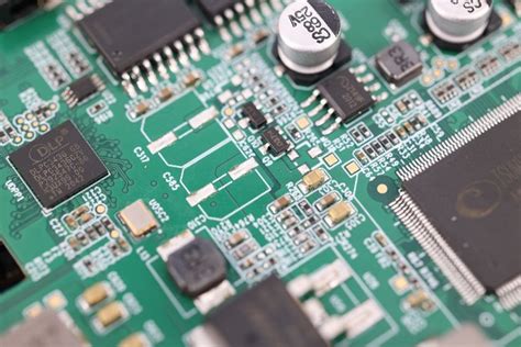
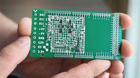
The PCB is essentially a flat board that houses and connects the various electronic components of the iPhone, including the processor, memory, and other critical elements.
It is composed of multiple layers of conductive and insulating materials, which are meticulously arranged to ensure efficient electrical connectivity and signal integrity.
One of the primary functions of the PCB in an iPhone is to provide a stable platform for mounting the device’s components.
This stability is crucial, as it ensures that the components remain securely in place, even when the phone is subjected to physical stress or movement. Moreover, the PCB facilitates the efficient routing of electrical signals between these components, enabling them to communicate and work together seamlessly. This is achieved through a complex network of copper traces and vias, which are carefully designed to minimize interference and signal loss.
In addition to its structural and electrical functions, the PCB also plays a critical role in thermal management within the iPhone.
As electronic components generate heat during operation, it is essential to dissipate this heat effectively to prevent overheating and ensure optimal performance. The PCB is designed with thermal management in mind, incorporating features such as thermal vias and heat sinks to facilitate the transfer of heat away from sensitive components. This helps to maintain the device’s temperature within safe limits, thereby enhancing its reliability and longevity.
Furthermore, the design of the PCB in an iPhone is a testament to the remarkable advancements in miniaturization and integration.
As smartphones have evolved, there has been a continuous push towards making devices thinner and more compact, without compromising on performance. The PCB has been at the forefront of this evolution, with manufacturers employing advanced techniques such as multi-layering and high-density interconnects to pack more functionality into a smaller space. This has allowed for the inclusion of more features and capabilities in each successive generation of the iPhone, while still maintaining a sleek and elegant form factor.
Moreover, the PCB’s role extends beyond just the physical and electrical aspects of the iPhone.
It also plays a crucial part in ensuring the device’s compliance with various regulatory standards and certifications. This involves rigorous testing and validation processes to ensure that the PCB meets the necessary electromagnetic compatibility (EMC) and safety requirements. By adhering to these standards, manufacturers can ensure that the iPhone operates safely and efficiently in a wide range of environments.
In conclusion, the PCB is an indispensable component in the design and functionality of the iPhone. Its role in providing structural support, facilitating electrical connectivity, managing thermal performance, and enabling miniaturization underscores its importance in the overall design of the device. As technology continues to advance, the PCB will undoubtedly remain a key focus of innovation, driving further improvements in smartphone performance and design. Understanding the intricacies of the PCB not only highlights its significance but also provides insight into the complex engineering that underpins modern smartphone technology.
Innovations In iPhone PCB Technology
The evolution of iPhone printed circuit board (PCB) technology has been a cornerstone in the advancement of smartphone capabilities, driving innovation and enhancing user experience. As the backbone of the device, the PCB is responsible for connecting various electronic components, enabling them to communicate and function seamlessly. Over the years, Apple has consistently pushed the boundaries of PCB technology, integrating cutting-edge advancements to improve performance, efficiency, and design.
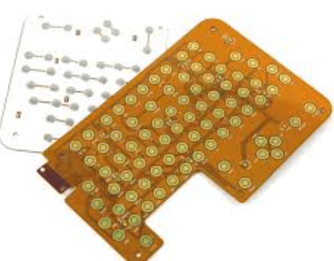
One of the most significant innovations in iPhone PCB technology is the transition to flexible PCBs.
Unlike traditional rigid PCBs, flexible PCBs offer enhanced durability and versatility, allowing for more compact and lightweight designs. This flexibility is crucial in accommodating the increasingly complex internal architecture of modern iPhones, where space is at a premium. By utilizing flexible PCBs, Apple can optimize the internal layout, ensuring that components are efficiently arranged to maximize performance while minimizing size.
Moreover, the introduction of multi-layer PCBs has been instrumental in supporting the sophisticated functionalities of iPhones.
Multi-layer PCBs consist of several layers of circuitry stacked together, allowing for more intricate and dense circuit designs. This innovation has enabled Apple to incorporate advanced features such as high-resolution displays, powerful processors, and enhanced connectivity options without compromising on the device’s slim profile. The ability to integrate multiple layers of circuitry has also improved signal integrity and reduced electromagnetic interference, resulting in a more reliable and efficient device.
In addition to structural advancements, material innovations have played a pivotal role in the evolution of iPhone PCBs.
Apple has increasingly focused on using environmentally friendly materials, aligning with its commitment to sustainability. By incorporating materials such as halogen-free laminates and lead-free solder, Apple not only reduces the environmental impact of its devices but also enhances the thermal and electrical performance of the PCBs. These materials are designed to withstand higher temperatures and provide better insulation, ensuring the longevity and reliability of the device.
Furthermore, the miniaturization of components has been a key driver of innovation in iPhone PCB technology.
As consumer demand for more powerful and feature-rich smartphones grows, Apple has had to find ways to pack more functionality into smaller spaces. This has led to the development of advanced manufacturing techniques, such as surface-mount technology (SMT), which allows for the placement of smaller components on the PCB. SMT has enabled Apple to increase the density of components on the PCB, resulting in more powerful and efficient devices without increasing their size.
Another noteworthy advancement is the integration of system-on-chip (SoC) technology into iPhone PCBs.
SoCs combine multiple functions, such as processing, memory, and connectivity, into a single chip, reducing the need for separate components. This integration not only saves space but also improves power efficiency and performance. By leveraging SoC technology, Apple can deliver faster processing speeds and enhanced graphics capabilities, providing users with a seamless and immersive experience.
In conclusion, the continuous innovation in iPhone PCB technology has been instrumental in shaping the capabilities and design of modern smartphones. Through advancements in flexible and multi-layer PCBs, material innovations, miniaturization of components, and the integration of SoC technology, Apple has consistently set new standards in the industry. As technology continues to evolve, it is likely that iPhone PCB technology will continue to advance, driving further innovation and enhancing the user experience.
Challenges In Manufacturing iPhone PCBs
The manufacturing of iPhone printed circuit boards (PCBs) presents a myriad of challenges that are both intricate and multifaceted. As the backbone of the device’s electronic architecture, PCBs are crucial for ensuring the seamless operation of the iPhone’s myriad functions. However, the journey from design to production is fraught with complexities that require precision, innovation, and stringent quality control.
To begin with, the miniaturization of components is a significant challenge in the manufacturing of iPhone PCBs.
As consumer demand for sleeker and more powerful devices grows, manufacturers are compelled to fit an increasing number of components into a smaller space. This necessitates the use of advanced technologies such as high-density interconnect (HDI) PCBs, which allow for more connections in a limited area. However, the implementation of HDI technology requires sophisticated equipment and expertise, which can drive up production costs and complicate the manufacturing process.
Moreover, the materials used in iPhone PCBs must meet rigorous standards to ensure durability and performance.
The choice of substrate material, for instance, is critical as it affects the board’s thermal and electrical properties. Manufacturers often opt for materials like FR-4, a composite of woven fiberglass cloth with an epoxy resin binder, which offers a good balance of performance and cost. However, as iPhones become more powerful, there is a growing need for materials that can withstand higher temperatures and offer better electrical insulation, further complicating the material selection process.
In addition to material challenges, the precision required in the etching and layering processes of PCB manufacturing cannot be overstated.
The etching process, which involves removing excess copper from the board to create the desired circuit patterns, must be executed with extreme accuracy to prevent defects that could compromise the board’s functionality. Similarly, the layering process, which involves stacking multiple layers of circuits, requires meticulous alignment to ensure that all connections are correctly established. Any misalignment can lead to short circuits or open circuits, which can render the PCB unusable.
Furthermore, the testing and quality assurance phase of iPhone PCB manufacturing is critical yet challenging.
Given the complexity of modern PCBs, comprehensive testing is essential to identify any defects or issues before the boards are assembled into the final product. This involves a range of tests, including electrical testing, thermal cycling, and visual inspections, all of which require specialized equipment and skilled personnel. The need for thorough testing is underscored by the high stakes involved; a single faulty PCB can lead to significant financial losses and damage to the brand’s reputation.
Finally, the environmental impact of PCB manufacturing is an ongoing concern.
The process involves the use of various chemicals and materials that can be harmful to the environment if not managed properly. As such, manufacturers are under increasing pressure to adopt sustainable practices, such as recycling waste materials and reducing energy consumption. This adds another layer of complexity to the manufacturing process, as companies must balance environmental responsibility with the need to maintain efficiency and cost-effectiveness.
In conclusion, the manufacturing of iPhone PCBs is a complex endeavor that involves navigating a host of challenges. From miniaturization and material selection to precision in production and environmental considerations, each aspect requires careful attention and expertise. As technology continues to evolve, manufacturers must remain agile and innovative to overcome these challenges and meet the ever-growing demands of the market.
The Future Of iPhone PCB Development
The future of iPhone PCB (Printed Circuit Board) development is poised to undergo significant transformations, driven by advancements in technology and the ever-evolving demands of consumers. As the backbone of electronic devices, PCBs play a crucial role in the functionality and performance of smartphones, including the iPhone. With each new iteration, Apple strives to enhance the capabilities of its devices, and the development of more sophisticated PCBs is central to this mission.
One of the primary trends shaping the future of iPhone PCB development is miniaturization.
As consumers demand sleeker and more compact devices, Apple is compelled to innovate in the design and manufacturing of PCBs. This involves reducing the size of components and optimizing the layout to fit more functionality into a smaller space. Advanced techniques such as high-density interconnect (HDI) technology are being employed to achieve this goal. HDI PCBs allow for more connections in a smaller area, enabling the integration of additional features without compromising the device’s form factor.
In addition to miniaturization, the push for enhanced performance is driving PCB development.
The need for faster processing speeds, improved energy efficiency, and better thermal management is paramount. To address these challenges, Apple is exploring the use of new materials and innovative design approaches. For instance, the incorporation of advanced substrates and the use of multi-layer PCBs can significantly improve signal integrity and reduce power consumption. These advancements not only enhance the performance of the iPhone but also contribute to a more sustainable product by extending battery life and reducing energy usage.
Moreover, the integration of 5G technology into iPhones necessitates further advancements in PCB design.
The high-frequency signals associated with 5G require PCBs that can support faster data transmission and lower latency. This demands meticulous attention to detail in the design and manufacturing processes to ensure that the PCBs can handle the increased demands of 5G networks. As a result, Apple is investing in research and development to create PCBs that can seamlessly support these next-generation communication standards.
Another significant factor influencing the future of iPhone PCB development is the growing emphasis on environmental sustainability.
As global awareness of environmental issues increases, Apple is committed to reducing the ecological footprint of its products. This commitment extends to the materials and processes used in PCB manufacturing. The company is exploring eco-friendly materials and sustainable manufacturing practices to minimize waste and reduce the use of hazardous substances. By prioritizing sustainability, Apple aims to create products that are not only technologically advanced but also environmentally responsible.
Furthermore, the rise of artificial intelligence (AI) and machine learning is expected to impact PCB development.
These technologies can be leveraged to optimize the design and testing of PCBs, leading to more efficient production processes and higher-quality products. AI-driven simulations and predictive analytics can identify potential issues early in the design phase, reducing the likelihood of costly errors and improving overall reliability.
In conclusion, the future of iPhone PCB development is characterized by a convergence of miniaturization, performance enhancement, 5G integration, sustainability, and AI-driven innovation. As Apple continues to push the boundaries of technology, the evolution of PCBs will play a pivotal role in shaping the capabilities and success of future iPhone models. Through ongoing research and development, Apple is poised to meet the challenges of tomorrow, delivering devices that are not only cutting-edge but also aligned with the values of a rapidly changing world.