How to design multilayer pcb
Understanding The Basics Of Multilayer PCB Design
Designing a multilayer printed circuit board (PCB) is a complex yet rewarding task that requires a thorough understanding of both the theoretical and practical aspects of electronics.
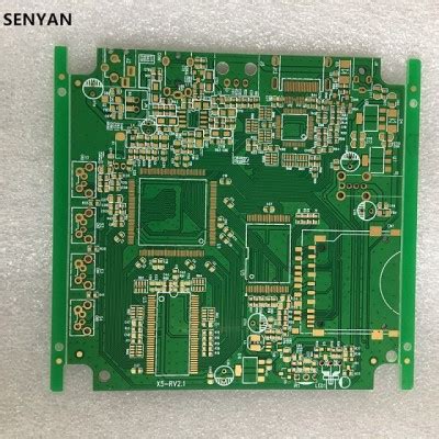
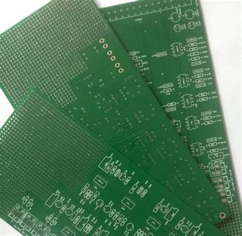
At its core, a multilayer PCB consists of multiple layers of conductive material, typically copper, separated by insulating layers, which are laminated together to form a single, cohesive unit.
This design allows for more complex and compact circuits, making it an essential component in modern electronic devices.
To begin with, it is crucial to understand the fundamental principles that govern multilayer PCB design.
The first step in designing a multilayer PCB is to determine the number of layers required.
This decision is influenced by several factors, including the complexity of the circuit, the number of connections needed, and the physical size constraints of the final product. Generally, more layers allow for greater routing flexibility and can help reduce electromagnetic interference (EMI) by providing dedicated ground and power planes. However, adding layers also increases the cost and complexity of manufacturing, so it is important to strike a balance between these considerations.
Once the number of layers is decided, the next step is to define the stack-up configuration.
The stack-up refers to the arrangement of conductive and insulating layers within the PCB. A well-designed stack-up can significantly improve the electrical performance of the board by minimizing signal integrity issues and reducing EMI. Typically, a multilayer PCB will have alternating layers of signal and plane (ground or power) layers. The placement of these layers should be carefully considered to ensure optimal performance. For instance, placing a ground plane adjacent to a signal layer can help shield the signals from external noise.
After establishing the stack-up, the focus shifts to the layout of the PCB.
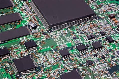
This involves placing components and routing traces on the various layers. Component placement is a critical aspect of PCB design, as it can impact the board’s functionality, manufacturability, and thermal performance. Components should be placed logically, with related components grouped together to minimize trace lengths and reduce potential interference. Additionally, attention should be paid to the orientation of components to facilitate efficient routing.
Routing, the process of connecting components with traces, is another crucial element of multilayer PCB design.
Effective routing requires careful planning to ensure that signals are transmitted with minimal loss and distortion. It is important to follow best practices, such as maintaining consistent trace widths, using vias judiciously, and avoiding sharp angles in traces. Furthermore, differential pairs and high-speed signals should be routed with particular care to maintain signal integrity.
In addition to these technical considerations, it is essential to adhere to design rules and standards throughout the PCB design process.
These rules, which can vary depending on the manufacturer and application, dictate parameters such as trace width, spacing, and via size. Compliance with these standards ensures that the PCB can be manufactured reliably and will perform as intended in its final application.
In conclusion, designing a multilayer PCB is a multifaceted process that requires a deep understanding of both the theoretical and practical aspects of electronics. By carefully considering factors such as layer count, stack-up configuration, component placement, and routing, designers can create efficient and reliable PCBs that meet the demands of modern electronic devices. As technology continues to advance, the importance of mastering multilayer PCB design will only grow, making it a valuable skill for any electronics engineer.
Key Considerations For Layer Stackup In Multilayer PCBs
Designing a multilayer printed circuit board (PCB) involves a complex interplay of various factors, with the layer stackup being one of the most critical elements.
The layer stackup not only influences the electrical performance of the PCB but also affects its mechanical stability, manufacturability, and cost.
Therefore, understanding the key considerations for layer stackup in multilayer PCBs is essential for engineers and designers aiming to optimize their designs.
To begin with, the number of layers in a PCB is a fundamental consideration.
The decision on the number of layers is typically driven by the complexity of the circuit, the need for signal integrity, and the space constraints of the final product. More layers allow for greater routing flexibility and can help in managing electromagnetic interference (EMI) by providing dedicated ground and power planes. However, increasing the number of layers also raises the cost and complexity of manufacturing. Thus, a balance must be struck between performance requirements and budgetary constraints.
In addition to the number of layers, the arrangement of these layers is crucial.
A well-thought-out layer stackup can significantly enhance signal integrity and reduce EMI. Typically, a multilayer PCB will have alternating signal and plane layers. Placing a ground plane adjacent to a signal layer can help in minimizing crosstalk and maintaining signal integrity. Moreover, having power and ground planes close together can create a low-inductance path, which is beneficial for high-speed designs.
The choice of materials for the layers is another important consideration.
The dielectric material between the layers affects the electrical properties of the PCB, such as impedance and signal propagation speed. Common materials include FR-4, which is widely used due to its good balance of performance and cost. However, for high-frequency applications, materials with lower dielectric constants and loss tangents, such as Rogers or Teflon, may be preferred. The selection of materials should align with the electrical requirements of the design as well as the thermal and mechanical demands of the application.
Furthermore, the thickness of each layer and the overall thickness of the PCB must be carefully planned.
The thickness impacts the board’s mechanical strength and its ability to dissipate heat. It also affects the impedance of the traces, which is critical for high-speed signal transmission. Designers must ensure that the layer thicknesses are compatible with the manufacturing capabilities of their chosen PCB fabricator.
Transitioning to the aspect of manufacturability, it is essential to consider the capabilities and limitations of the PCB manufacturer during the design phase.
Different manufacturers may have varying capabilities in terms of minimum trace widths, spacing, and via sizes. Engaging with the manufacturer early in the design process can help in aligning the design with manufacturing capabilities, thereby reducing the risk of costly redesigns.
Finally, cost considerations cannot be overlooked.
While a more complex stackup with advanced materials and additional layers can offer superior performance, it also increases the cost. Designers must evaluate the trade-offs between performance and cost to ensure that the final product meets both technical and financial objectives.
In conclusion, designing a multilayer PCB requires careful consideration of various factors related to the layer stackup. By thoughtfully addressing the number of layers, their arrangement, material selection, thickness, manufacturability, and cost, designers can create PCBs that meet the desired performance criteria while remaining within budget. This holistic approach to layer stackup is essential for the successful development of modern electronic devices.
Best Practices For Signal Integrity In Multilayer PCB Design
Designing multilayer printed circuit boards (PCBs) requires a meticulous approach to ensure signal integrity, which is crucial for the performance and reliability of electronic devices. Signal integrity refers to the quality and reliability of electrical signals as they travel through the PCB. Poor signal integrity can lead to data errors, electromagnetic interference, and overall system failure. Therefore, understanding and implementing best practices for signal integrity in multilayer PCB design is essential.
To begin with, one of the fundamental aspects of maintaining signal integrity is the careful planning of the layer stack-up.
The stack-up configuration significantly influences the electrical performance of the PCB. A well-designed stack-up minimizes electromagnetic interference and crosstalk between layers. Typically, a balanced stack-up with alternating signal and ground planes is recommended. This configuration provides a controlled impedance environment, which is vital for high-speed signal transmission.
Moreover, the placement of components plays a critical role in signal integrity.
Components should be strategically placed to minimize the length of signal paths, thereby reducing the potential for signal degradation. It is advisable to place high-speed components close to each other and to the relevant connectors. This proximity reduces the loop area and, consequently, the inductance, which can adversely affect signal quality.
In addition to component placement, trace routing is another crucial factor.
Traces should be routed with care to avoid sharp angles, which can cause signal reflections and impedance discontinuities. Instead, use smooth, gradual curves for trace routing. Furthermore, maintaining consistent trace width and spacing is essential to ensure uniform impedance. Differential pairs, which are commonly used for high-speed signals, should be routed together with equal lengths to prevent skew and maintain signal integrity.
Ground planes are indispensable in multilayer PCB design for providing a return path for signals and reducing electromagnetic interference.
It is important to ensure that ground planes are continuous and unbroken. Any gaps or splits in the ground plane can lead to increased loop inductance and potential signal integrity issues. Additionally, stitching vias can be used to connect ground planes across different layers, further enhancing signal integrity by providing multiple return paths.
Signal integrity can also be improved by using proper termination techniques.
Termination resistors can be employed to match the impedance of the transmission line to the load, thereby minimizing reflections. The choice of termination method, whether series or parallel, depends on the specific application and signal characteristics.
Furthermore, power integrity is closely related to signal integrity. A stable power distribution network is essential for maintaining signal quality.
Decoupling capacitors should be placed close to power pins to filter out noise and provide a stable voltage supply. The use of multiple power and ground planes can also help in reducing power supply noise and improving overall signal integrity.
Finally, simulation and analysis tools are invaluable in the design process. These tools allow designers to model and predict the behavior of signals within the PCB, enabling the identification and mitigation of potential signal integrity issues before physical prototyping. By leveraging these tools, designers can optimize the PCB layout for maximum performance and reliability.
In conclusion, ensuring signal integrity in multilayer PCB design involves a comprehensive approach that includes careful layer stack-up planning, strategic component placement, meticulous trace routing, continuous ground planes, proper termination, and robust power distribution. By adhering to these best practices, designers can create PCBs that deliver reliable and high-quality performance in complex electronic systems.
Advanced Techniques For Thermal Management In Multilayer PCBs
Designing multilayer printed circuit boards (PCBs) involves a complex interplay of various factors, among which thermal management stands out as a critical consideration. As electronic devices become more compact and powerful, the heat generated by components can significantly impact performance and reliability. Therefore, advanced techniques for thermal management in multilayer PCBs are essential to ensure optimal functionality and longevity.
To begin with, understanding the thermal properties of materials used in PCB construction is fundamental.
The choice of substrate material, such as FR-4, polyimide, or ceramic, can influence the thermal conductivity and overall heat dissipation capabilities of the board. For instance, ceramic substrates offer superior thermal conductivity compared to traditional FR-4, making them suitable for high-power applications. By selecting materials with appropriate thermal properties, designers can enhance the board’s ability to manage heat effectively.
In addition to material selection, the layout of the PCB plays a pivotal role in thermal management.
Strategically placing heat-generating components and ensuring adequate spacing between them can prevent localized hotspots. Moreover, incorporating thermal vias—small holes filled with conductive material—can facilitate heat transfer from the surface layers to the inner layers or to a heat sink. This technique is particularly useful in multilayer PCBs, where heat can be dissipated across multiple layers, thereby reducing the thermal load on any single layer.
Furthermore, the use of copper planes within the PCB can significantly aid in heat distribution.
Copper, with its high thermal conductivity, can act as a heat spreader, distributing heat evenly across the board. By designing power and ground planes with sufficient thickness and area, designers can create effective thermal pathways that mitigate the risk of overheating.
Additionally, employing thermal relief patterns around vias and pads can help balance the need for electrical connectivity with thermal management, ensuring that heat is efficiently conducted away from critical components.
Another advanced technique involves the integration of thermal management components such as heat sinks and thermal pads.
Heat sinks, typically made of aluminum or copper, can be attached to high-power components to dissipate heat into the surrounding environment. Thermal pads, on the other hand, provide a conductive interface between components and heat sinks, enhancing thermal transfer. By incorporating these elements into the PCB design, engineers can further improve the board’s ability to manage heat.
Moreover, simulation tools have become invaluable in the design process, allowing engineers to model and predict thermal behavior before physical prototypes are built.
These tools can simulate various scenarios, helping designers identify potential thermal issues and optimize the layout accordingly. By leveraging simulation software, designers can make informed decisions about component placement, layer stack-up, and thermal via distribution, ultimately leading to more efficient thermal management.
In conclusion, advanced techniques for thermal management in multilayer PCBs are crucial for ensuring the performance and reliability of modern electronic devices. By carefully selecting materials, optimizing layout, utilizing copper planes, integrating thermal components, and employing simulation tools, designers can effectively address the challenges posed by heat generation. As technology continues to evolve, the importance of robust thermal management strategies in PCB design will only grow, underscoring the need for ongoing innovation and expertise in this field.