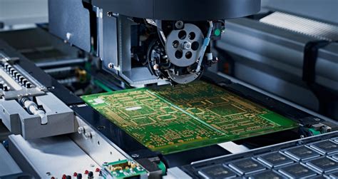
High speed serial and parallel buses on pcb layout cadence
Optimizing Signal Integrity in High-Speed Serial Buses on PCB Layouts
In the realm of modern electronics, the demand for faster data transmission has led to the widespread adoption of high-speed serial buses in printed circuit board (PCB) layouts. These buses, which include standards such as PCIe, USB, and SATA, are integral to the performance of contemporary electronic devices. As data rates increase, ensuring signal integrity becomes a critical challenge for engineers. Signal integrity refers to the quality and reliability of electrical signals as they travel through the PCB, and it is influenced by various factors such as impedance mismatches, crosstalk, and electromagnetic interference. Therefore, optimizing signal integrity in high-speed serial buses is essential for maintaining the functionality and efficiency of electronic systems.
One of the primary considerations in optimizing signal integrity is the careful design of the PCB layout.
The layout must be meticulously planned to minimize impedance discontinuities, which can cause signal reflections and degrade signal quality. To achieve this, designers often employ controlled impedance traces, which involve maintaining a consistent trace width and spacing to ensure uniform impedance throughout the signal path. Additionally, the use of differential signaling, where two complementary signals are transmitted simultaneously, can help reduce susceptibility to external noise and improve signal integrity.
Moreover, the placement of components on the PCB plays a crucial role in signal integrity.
Components should be strategically positioned to minimize the length of high-speed traces, thereby reducing the potential for signal degradation. Furthermore, the use of ground planes and power planes can provide a low-inductance return path for signals, which is vital for maintaining signal integrity at high frequencies. These planes also help in reducing electromagnetic interference by providing effective shielding.
Transitioning to the topic of crosstalk, it is another significant factor that can adversely affect signal integrity in high-speed serial buses.
Crosstalk occurs when a signal in one trace induces an unwanted signal in an adjacent trace, leading to data corruption. To mitigate crosstalk, designers can increase the spacing between traces or employ guard traces, which are grounded traces placed between signal lines to absorb interference. Additionally, using a multi-layer PCB design can help separate high-speed signals from other traces, further reducing the risk of crosstalk.
In addition to layout considerations, the choice of materials is also pivotal in optimizing signal integrity.
High-frequency laminates with low dielectric constant and low loss tangent are preferred for high-speed applications, as they minimize signal attenuation and dispersion. These materials help maintain signal integrity over longer distances and at higher frequencies, which is essential for the reliable operation of high-speed serial buses.
Furthermore, simulation tools such as Cadence’s PCB design software can be invaluable in optimizing signal integrity.
These tools allow designers to model and analyze the electrical performance of their PCB layouts before fabrication, enabling them to identify and address potential signal integrity issues early in the design process. By simulating various scenarios and configurations, designers can make informed decisions about trace routing, component placement, and material selection, ultimately enhancing the performance of high-speed serial buses.
In conclusion, optimizing signal integrity in high-speed serial buses on PCB layouts is a multifaceted challenge that requires careful consideration of layout design, component placement, material selection, and the use of advanced simulation tools. By addressing these factors, engineers can ensure the reliable transmission of data in high-speed electronic systems, thereby meeting the ever-increasing demands of modern technology.
Design Techniques for Parallel Bus Routing in Cadence PCB Layout
In the realm of printed circuit board (PCB) design, the efficient routing of high-speed serial and parallel buses is a critical aspect that demands meticulous attention. As technology advances, the need for faster data transmission rates has become paramount, necessitating the use of sophisticated design techniques to ensure signal integrity and optimal performance. Cadence PCB layout tools offer a robust platform for addressing these challenges, providing designers with the necessary resources to implement effective routing strategies for parallel buses.
To begin with, understanding the fundamental differences between serial and parallel buses is essential.
While serial buses transmit data sequentially over a single channel, parallel buses send multiple bits simultaneously across multiple channels. This inherent difference necessitates distinct design approaches, particularly when it comes to routing on a PCB. In the context of parallel bus routing, maintaining signal integrity is a primary concern, as the simultaneous transmission of multiple signals can lead to issues such as crosstalk and signal skew.
One of the key techniques employed in parallel bus routing is the use of controlled impedance traces.
By carefully designing the width and spacing of traces, designers can ensure that the impedance remains consistent, thereby minimizing reflections and signal degradation. Cadence PCB layout tools facilitate this process by providing impedance calculators and design rule checks that help maintain the desired electrical characteristics throughout the routing process.
Moreover, length matching is another critical consideration in parallel bus routing.
To prevent signal skew, which can occur when signals arrive at their destination at different times, it is imperative to ensure that all traces in a parallel bus are of equal length. Cadence tools offer automated length matching features that allow designers to easily adjust trace lengths, ensuring that timing requirements are met without compromising the overall layout.
In addition to these techniques, the strategic placement of vias and the use of differential pairs can further enhance the performance of parallel buses.
Vias, which are used to connect different layers of a PCB, can introduce unwanted inductance and capacitance if not placed judiciously. By minimizing the number of vias and optimizing their placement, designers can reduce potential signal integrity issues. Furthermore, employing differential pairs, where two complementary signals are routed together, can help mitigate the effects of electromagnetic interference and improve noise immunity.
Transitioning from design considerations to practical implementation, Cadence PCB layout tools offer a suite of features that streamline the routing process.
The interactive routing capabilities allow designers to visualize and adjust trace paths in real-time, while the constraint-driven environment ensures that all design rules are adhered to. Additionally, the integration of simulation tools enables designers to validate their designs before fabrication, identifying potential issues and making necessary adjustments early in the design cycle.
In conclusion, the routing of high-speed parallel buses on a PCB is a complex task that requires a comprehensive understanding of both electrical and physical design principles. By leveraging the advanced features of Cadence PCB layout tools, designers can effectively address the challenges associated with parallel bus routing, ensuring that their designs meet the stringent requirements of modern high-speed applications. Through careful planning and the application of proven design techniques, it is possible to achieve optimal performance and reliability in high-speed PCB designs.
Managing Crosstalk in High-Speed Serial and Parallel Buses
In the realm of printed circuit board (PCB) design, managing crosstalk in high-speed serial and parallel buses is a critical consideration that can significantly impact the performance and reliability of electronic systems. As data rates continue to escalate, the challenges associated with crosstalk become more pronounced, necessitating meticulous attention to detail during the PCB layout process.
Crosstalk, which refers to the unwanted coupling of signals between adjacent traces, can lead to signal integrity issues, data corruption, and ultimately, system failure.
Therefore, understanding and mitigating crosstalk is essential for ensuring the optimal functioning of high-speed buses.
To begin with, it is important to recognize the factors that contribute to crosstalk in high-speed environments.
The proximity of traces, the dielectric properties of the PCB material, and the frequency of the signals all play a role in the extent of crosstalk experienced. In high-speed serial buses, where data is transmitted over a single channel at a time, the risk of crosstalk is often lower compared to parallel buses. However, as data rates increase, even serial buses are not immune to crosstalk issues. On the other hand, parallel buses, which transmit multiple bits simultaneously across several channels, are inherently more susceptible to crosstalk due to the close proximity of the traces.
One effective strategy for managing crosstalk is to optimize the physical layout of the PCB.
This involves carefully planning the routing of traces to minimize their length and maintain adequate spacing between them. By increasing the distance between adjacent traces, the potential for electromagnetic interference is reduced, thereby mitigating crosstalk. Additionally, employing differential signaling, where two complementary signals are transmitted over a pair of traces, can help cancel out noise and further reduce crosstalk. This technique is particularly beneficial in high-speed serial buses, where maintaining signal integrity is paramount.
Moreover, the use of ground planes and shielding can significantly aid in crosstalk reduction.
Ground planes provide a low-impedance return path for signals, which helps to contain electromagnetic fields and minimize their impact on neighboring traces. In parallel buses, where multiple signals are transmitted simultaneously, incorporating ground traces between signal lines can act as a barrier to crosstalk. Similarly, using shielding techniques, such as enclosing traces in a conductive material, can effectively isolate signals and prevent unwanted coupling.
In addition to physical layout considerations, selecting the appropriate PCB materials is crucial for managing crosstalk.
Materials with low dielectric constants and low loss tangents are preferred, as they reduce signal attenuation and dispersion, thereby preserving signal integrity. Furthermore, employing advanced simulation tools during the design phase can provide valuable insights into potential crosstalk issues. These tools allow designers to model and analyze the electromagnetic behavior of the PCB, enabling them to identify and address crosstalk concerns before the physical board is fabricated.
In conclusion, managing crosstalk in high-speed serial and parallel buses is a multifaceted challenge that requires a comprehensive approach.
By optimizing the physical layout, utilizing differential signaling, incorporating ground planes and shielding, and selecting appropriate materials, designers can effectively mitigate crosstalk and ensure the reliable performance of high-speed buses. As data rates continue to rise, the importance of addressing crosstalk in PCB design will only grow, underscoring the need for ongoing innovation and attention to detail in this critical aspect of electronic design.
Best Practices for Power Distribution in High-Speed Bus Designs
In the realm of high-speed serial and parallel bus designs on printed circuit boards (PCBs), effective power distribution is paramount to ensure optimal performance and reliability. As data rates continue to escalate, the challenges associated with power integrity become increasingly complex. Therefore, understanding and implementing best practices for power distribution is essential for engineers working with high-speed bus designs in PCB layout tools like Cadence.
To begin with, one of the fundamental aspects of power distribution in high-speed bus designs is the minimization of power supply noise.
This can be achieved through the strategic placement of decoupling capacitors. These capacitors serve to stabilize the power supply by providing a local energy reservoir, which helps to mitigate voltage fluctuations caused by rapid changes in current demand. It is advisable to place decoupling capacitors as close as possible to the power pins of integrated circuits. This proximity reduces the inductive effects of the power delivery network, thereby enhancing the effectiveness of the capacitors.
Moreover, the selection of appropriate capacitor values is crucial.
A combination of capacitors with different values can be employed to cover a wide frequency range, ensuring that both high-frequency and low-frequency noise components are adequately filtered. Typically, larger capacitors are effective at filtering low-frequency noise, while smaller capacitors are better suited for high-frequency noise. By using a mix of capacitor values, engineers can create a robust power distribution network that addresses a broad spectrum of noise issues.
In addition to decoupling strategies, the design of power and ground planes plays a significant role in power distribution.
A well-designed power plane can reduce impedance and improve current distribution across the PCB. It is recommended to use solid power and ground planes rather than traces, as planes provide a lower impedance path for current flow. This is particularly important in high-speed designs where even small impedance variations can lead to significant performance degradation.
Furthermore, maintaining a low inductance path between power and ground planes is essential.
This can be achieved by minimizing the distance between these planes, which reduces the loop inductance and enhances the overall power integrity. In Cadence PCB layout tools, designers can utilize features such as via stitching to create multiple connections between power and ground planes, further reducing inductance and improving current return paths.
Another best practice involves the careful routing of high-speed signals to minimize crosstalk and electromagnetic interference (EMI).
High-speed buses are susceptible to these issues, which can be exacerbated by poor power distribution. By ensuring that power and ground planes are properly designed and that signal traces are routed with adequate spacing and shielding, engineers can mitigate the adverse effects of crosstalk and EMI.
Finally, simulation and analysis tools available in Cadence can be invaluable in verifying power distribution network performance.
These tools allow engineers to model and simulate the power integrity of their designs, identifying potential issues before physical prototyping. By leveraging these capabilities, designers can optimize their power distribution strategies, ensuring that high-speed bus designs meet the stringent requirements of modern electronic systems.
In conclusion, effective power distribution is a critical component of high-speed serial and parallel bus designs on PCBs. By employing best practices such as strategic decoupling, careful plane design, and thorough simulation, engineers can enhance power integrity and ensure the reliable operation of their high-speed designs. As technology continues to advance, these practices will remain essential in meeting the demands of increasingly complex electronic systems.