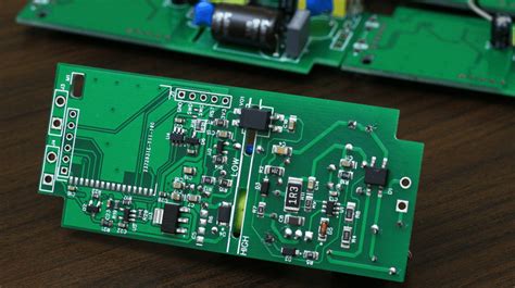
High speed rf pcb design
Challenges In High-Speed RF PCB Design
High-speed RF PCB design presents a unique set of challenges that require careful consideration and meticulous planning. As the demand for faster and more efficient electronic devices continues to grow, engineers are tasked with overcoming the complexities associated with designing printed circuit boards (PCBs) that can handle high-frequency signals.
One of the primary challenges in high-speed RF PCB design is managing signal integrity.
At high frequencies, even the smallest imperfections in the PCB layout can lead to significant signal degradation. This is due to the fact that high-speed signals are more susceptible to issues such as crosstalk, reflection, and electromagnetic interference (EMI). To mitigate these problems, designers must pay close attention to trace routing, impedance matching, and the use of proper grounding techniques.
Moreover, the choice of materials plays a crucial role in high-speed RF PCB design.
Traditional FR-4 substrates, commonly used in standard PCB manufacturing, may not provide the necessary performance for high-frequency applications. Instead, materials with lower dielectric constants and loss tangents, such as Rogers or Teflon-based laminates, are often preferred. These materials help to minimize signal loss and ensure that the PCB can support the desired frequency range. However, the use of specialized materials can also increase the cost and complexity of the manufacturing process, posing an additional challenge for designers.
Thermal management is another critical aspect of high-speed RF PCB design.
As the frequency of operation increases, so does the power consumption and heat generation within the circuit. Effective thermal management is essential to prevent overheating, which can lead to component failure and reduced reliability. Designers must incorporate adequate heat dissipation techniques, such as the use of thermal vias, heat sinks, and proper airflow management, to ensure the longevity and performance of the PCB.
Furthermore, the miniaturization of electronic components adds another layer of complexity to high-speed RF PCB design.
As devices become smaller and more compact, the available space for routing traces and placing components becomes increasingly limited. This necessitates the use of advanced design techniques, such as microvias and blind/buried vias, to maximize the use of available space while maintaining signal integrity. Additionally, the integration of multiple functions into a single PCB can lead to increased electromagnetic interference, requiring designers to implement effective shielding and isolation strategies.
In addition to these technical challenges, high-speed RF PCB design also demands a thorough understanding of regulatory and compliance requirements.
Different regions and industries have specific standards that must be adhered to, such as those set by the Federal Communications Commission (FCC) in the United States or the European Telecommunications Standards Institute (ETSI) in Europe. Ensuring compliance with these standards is crucial to avoid costly redesigns and delays in bringing products to market.
In conclusion, high-speed RF PCB design is a complex and multifaceted process that requires a deep understanding of various technical and regulatory factors. By addressing challenges related to signal integrity, material selection, thermal management, miniaturization, and compliance, designers can create PCBs that meet the demands of modern high-frequency applications. As technology continues to evolve, the ability to effectively navigate these challenges will be essential for engineers seeking to develop cutting-edge electronic devices.

Material Selection For High-Speed RF PCBs
In the realm of high-speed RF PCB design, material selection plays a pivotal role in determining the performance and reliability of the final product. As the demand for faster and more efficient electronic devices continues to grow, engineers are increasingly tasked with selecting materials that can support high-frequency signals while minimizing losses and maintaining signal integrity. The choice of substrate material is particularly crucial, as it directly impacts the electrical, thermal, and mechanical properties of the PCB.
To begin with, one must consider the dielectric constant (Dk) of the substrate material.
A lower dielectric constant is generally preferred for high-speed RF applications because it allows for faster signal propagation and reduces signal delay. Materials such as PTFE (polytetrafluoroethylene) and certain ceramic-filled laminates are often chosen for their low Dk values. However, it is essential to balance this with other factors, such as the material’s dissipation factor (Df), which measures the dielectric losses within the substrate. A low dissipation factor is desirable to minimize energy loss and ensure efficient signal transmission.
Moreover, the thermal properties of the substrate material cannot be overlooked.
High-speed RF circuits often generate significant heat, which can affect performance and reliability if not properly managed. Therefore, materials with high thermal conductivity are advantageous as they facilitate efficient heat dissipation. Additionally, the coefficient of thermal expansion (CTE) should be considered, especially in applications where the PCB will undergo temperature fluctuations. A substrate with a CTE that closely matches that of the copper traces can help prevent mechanical stress and potential failure.
Another critical aspect of material selection is the substrate’s ability to support fine line widths and spacing, which are often required in high-speed RF designs to accommodate the compact nature of modern electronic devices. Advanced materials that offer excellent dimensional stability and low moisture absorption are preferred, as they ensure consistent performance and prevent issues such as warping or delamination.
Furthermore, cost considerations also play a significant role in material selection.
While high-performance materials like PTFE and ceramic-filled laminates offer superior electrical and thermal properties, they can be significantly more expensive than traditional FR-4 substrates. Engineers must weigh the benefits of these advanced materials against their cost, considering the specific requirements and budget constraints of the project.
In addition to these factors, the manufacturability of the chosen material is also crucial.
Some high-performance materials may require specialized processing techniques, which can increase production complexity and cost. Therefore, it is important to collaborate closely with PCB manufacturers to ensure that the selected material can be effectively processed and that the final product meets the desired specifications.
In conclusion, selecting the appropriate material for high-speed RF PCB design is a complex process that involves balancing various electrical, thermal, mechanical, and economic factors. By carefully considering the dielectric constant, dissipation factor, thermal properties, and manufacturability of potential materials, engineers can optimize the performance and reliability of their high-speed RF circuits. As technology continues to advance, the development of new materials and fabrication techniques will undoubtedly play a key role in meeting the ever-increasing demands of high-speed electronic applications.
Signal Integrity Considerations In High-Speed RF PCB Design
In the realm of high-speed RF PCB design, signal integrity emerges as a pivotal consideration, demanding meticulous attention to detail and a comprehensive understanding of the underlying principles. As the frequency of operation increases, the challenges associated with maintaining signal integrity become more pronounced, necessitating a strategic approach to design and layout. At the core of these challenges lies the need to minimize signal degradation, which can manifest in various forms such as signal loss, distortion, and unwanted electromagnetic interference.
To begin with, one of the primary factors influencing signal integrity in high-speed RF PCB design is the choice of materials.
The dielectric constant and loss tangent of the substrate material play a crucial role in determining the propagation characteristics of RF signals. Materials with low dielectric constants and loss tangents are preferred as they reduce signal attenuation and dispersion, thereby preserving the integrity of the transmitted signals. Furthermore, the selection of appropriate materials can mitigate issues related to impedance mismatches, which are a common source of signal reflections and distortions.
In addition to material selection, the physical layout of the PCB is equally critical.
The routing of traces must be carefully planned to minimize parasitic inductance and capacitance, which can adversely affect signal integrity. For instance, maintaining consistent trace widths and spacing helps in achieving controlled impedance, which is essential for high-speed signal transmission. Moreover, the use of ground planes and power planes can significantly enhance signal integrity by providing a low-inductance return path and reducing electromagnetic interference.
Transitioning to another vital aspect, the management of crosstalk is indispensable in high-speed RF PCB design.
Crosstalk, which occurs when signals in adjacent traces interfere with each other, can lead to data corruption and signal degradation. To mitigate crosstalk, designers can employ techniques such as increasing the spacing between traces, using differential signaling, and implementing guard traces. These strategies help in isolating signals and minimizing the coupling between adjacent traces, thereby preserving signal integrity.
Furthermore, the consideration of via design is paramount in maintaining signal integrity.
Vias, which are used to connect different layers of a PCB, can introduce unwanted inductance and capacitance, leading to signal reflections and losses. To address this, designers can opt for techniques such as back-drilling, which removes the unused portion of a via, thereby reducing its parasitic effects. Additionally, the use of blind and buried vias can help in optimizing the signal path and minimizing disruptions.
As we delve deeper into the intricacies of high-speed RF PCB design, it becomes evident that power integrity is closely intertwined with signal integrity.
Ensuring a stable power delivery network is essential for maintaining signal integrity, as fluctuations in power supply can lead to jitter and timing errors. Implementing decoupling capacitors and designing an efficient power distribution network are effective strategies for enhancing power integrity, which in turn supports robust signal transmission.
In conclusion, signal integrity considerations in high-speed RF PCB design encompass a multitude of factors, each contributing to the overall performance and reliability of the system. By carefully selecting materials, optimizing layout, managing crosstalk, and ensuring power integrity, designers can effectively address the challenges associated with high-speed RF applications. As technology continues to advance, the importance of signal integrity in RF PCB design will only grow, underscoring the need for continued innovation and expertise in this critical field.

Advanced Techniques For High-Speed RF PCB Layout
In the realm of high-speed RF PCB design, the pursuit of optimal performance necessitates a meticulous approach to layout techniques. As the demand for faster and more efficient electronic devices continues to escalate, engineers are compelled to adopt advanced strategies that address the unique challenges posed by high-frequency signals. One of the fundamental considerations in high-speed RF PCB design is the management of signal integrity. Ensuring that signals maintain their integrity as they traverse the PCB is paramount, as any degradation can lead to significant performance issues. To achieve this, designers must pay close attention to trace geometry, impedance matching, and the minimization of parasitic elements.
Transitioning from signal integrity, another critical aspect is the control of electromagnetic interference (EMI).
High-speed RF circuits are particularly susceptible to EMI, which can emanate from both internal and external sources. To mitigate these effects, designers often employ techniques such as careful component placement, the use of ground planes, and the implementation of shielding. By strategically placing components and utilizing ground planes, designers can create a controlled environment that minimizes the potential for interference. Additionally, shielding can be employed to protect sensitive components from external EMI sources, further enhancing the overall performance of the PCB.
Moreover, power integrity is an essential consideration in high-speed RF PCB design.
Ensuring that power delivery networks (PDNs) are capable of supplying stable and noise-free power to all components is crucial. This involves the use of decoupling capacitors, which help to filter out noise and provide a stable power supply. Furthermore, the layout of power and ground planes must be carefully designed to minimize inductance and resistance, thereby reducing the potential for power fluctuations that could adversely affect the performance of the RF circuit.
In addition to these considerations, thermal management plays a pivotal role in high-speed RF PCB design.
As components operate at higher frequencies, they tend to generate more heat, which can lead to thermal issues if not properly managed. Effective thermal management strategies include the use of thermal vias, heat sinks, and thermal pads, which help to dissipate heat away from critical components. By ensuring that heat is efficiently managed, designers can prevent thermal-related failures and maintain the reliability of the PCB.
Furthermore, the choice of materials is a crucial factor in high-speed RF PCB design.
The dielectric properties of the substrate material can significantly impact signal propagation and loss. Therefore, selecting materials with low dielectric constant and low loss tangent is essential for maintaining signal integrity at high frequencies. Additionally, the use of advanced materials such as low-loss laminates can further enhance the performance of the PCB by reducing signal attenuation and improving overall efficiency.
In conclusion, high-speed RF PCB design is a complex and multifaceted discipline that requires a comprehensive understanding of various advanced techniques.
By focusing on signal integrity, EMI control, power integrity, thermal management, and material selection, designers can create PCBs that meet the demanding requirements of modern high-speed applications. As technology continues to evolve, the importance of these advanced techniques will only grow, underscoring the need for engineers to stay abreast of the latest developments in the field. Through careful planning and execution, high-speed RF PCB design can achieve the performance and reliability necessary for the next generation of electronic devices.