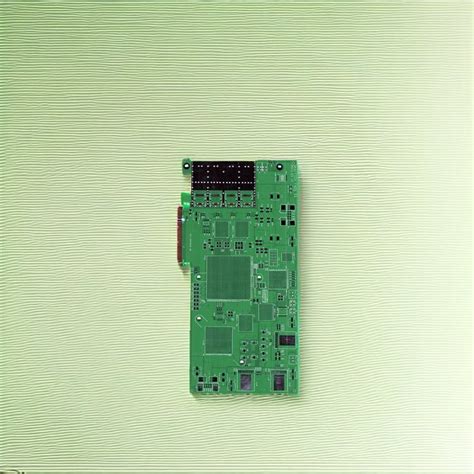
High speed pcb via
Optimizing Signal Integrity in High-Speed PCB Vias
In the realm of high-speed printed circuit board (PCB) design, optimizing signal integrity is paramount to ensuring the reliable performance of electronic devices. One critical aspect of this optimization process is the design and implementation of vias, which are the conductive pathways that allow signals to traverse different layers of a PCB. As data rates increase and electronic devices become more complex, the role of vias in maintaining signal integrity becomes increasingly significant. Therefore, understanding the intricacies of high-speed PCB vias is essential for engineers aiming to minimize signal degradation and electromagnetic interference.
To begin with, it is important to recognize that vias introduce discontinuities in the signal path, which can lead to reflections, crosstalk, and other forms of signal distortion.
These issues are particularly pronounced in high-speed applications where the wavelength of the signal approaches the physical dimensions of the via. Consequently, careful consideration must be given to the via design to mitigate these adverse effects. One effective strategy is to minimize the via stub, which is the portion of the via that extends beyond the signal layer. By reducing the stub length, engineers can significantly decrease the inductance and capacitance associated with the via, thereby enhancing signal integrity.
Moreover, the choice of via type plays a crucial role in optimizing signal integrity.
Traditional through-hole vias, while robust, can introduce substantial parasitic effects due to their extended length. In contrast, blind and buried vias offer a more refined solution by connecting only specific layers, thus reducing unnecessary via length and associated parasitics. Additionally, microvias, which are smaller in diameter and depth, provide an even more efficient means of interlayer connection, particularly in high-density interconnect (HDI) designs. These advanced via technologies not only improve signal integrity but also allow for greater design flexibility and miniaturization.
In addition to via type and stub length, the placement and distribution of vias on the PCB are critical factors in maintaining signal integrity.
Vias should be strategically placed to minimize their impact on the signal path and to avoid creating resonant structures that can exacerbate signal distortion. Furthermore, the use of ground vias adjacent to signal vias can help to shield the signal from electromagnetic interference and reduce crosstalk between adjacent traces. This practice, known as via stitching, is particularly effective in high-speed designs where maintaining a controlled impedance environment is essential.
Another consideration in optimizing high-speed PCB vias is the use of simulation tools to model and predict the behavior of signals as they traverse the via structure.
Electromagnetic simulation software can provide valuable insights into the potential impact of via design choices on signal integrity, allowing engineers to make informed decisions and optimize their designs before physical prototyping. By leveraging these tools, designers can identify potential issues early in the design process and implement corrective measures to ensure optimal performance.
In conclusion, optimizing signal integrity in high-speed PCB vias is a multifaceted challenge that requires careful consideration of via design, type, placement, and simulation. By addressing these factors, engineers can effectively mitigate the adverse effects of vias on signal integrity, thereby enhancing the performance and reliability of high-speed electronic devices. As technology continues to advance and data rates increase, the importance of optimizing PCB vias will only grow, underscoring the need for continued innovation and refinement in this critical area of electronic design.
Design Techniques for Minimizing Crosstalk in High-Speed PCB Vias
In the realm of high-speed printed circuit board (PCB) design, minimizing crosstalk is a critical consideration, particularly when dealing with vias. Vias, which are the conductive pathways that allow signals to traverse different layers of a PCB, can inadvertently become sources of electromagnetic interference if not properly managed. As signal speeds increase, the potential for crosstalk—unwanted coupling between signal paths—becomes more pronounced, necessitating careful design techniques to mitigate its effects.
To begin with, understanding the nature of crosstalk in high-speed environments is essential.
Crosstalk occurs when a signal in one trace induces an unwanted signal in an adjacent trace, primarily due to capacitive and inductive coupling. In high-speed PCBs, where signal rise times are fast and trace lengths are often long, the risk of crosstalk is exacerbated. Vias, by their very nature, introduce discontinuities in the signal path, which can lead to reflections and increased electromagnetic interference. Therefore, addressing these discontinuities is paramount in minimizing crosstalk.
One effective technique for reducing crosstalk in high-speed PCB vias is to optimize the via design itself.
This can be achieved by minimizing the via stub length, which is the portion of the via that extends beyond the signal layer. Long via stubs can act as antennas, radiating unwanted signals and increasing the potential for crosstalk. By employing back-drilling or controlled-depth drilling, designers can remove these stubs, thereby reducing their impact on signal integrity.
In addition to optimizing via design, careful consideration of trace routing is crucial.
Ensuring adequate spacing between traces can significantly reduce capacitive coupling, one of the primary contributors to crosstalk. The use of differential pairs, where two complementary signals are routed closely together, can also help mitigate crosstalk. This technique takes advantage of the fact that any noise induced in one trace is likely to be induced equally in the other, allowing the differential receiver to effectively cancel out the noise.
Moreover, the implementation of ground vias and stitching vias can further enhance signal integrity.
Ground vias provide a return path for signals, reducing loop area and minimizing inductive coupling. Stitching vias, placed strategically around signal vias, can help contain electromagnetic fields and prevent them from coupling into adjacent traces. These techniques, when used in conjunction with proper via design and trace routing, can significantly reduce the risk of crosstalk.
Furthermore, the choice of materials and layer stack-up plays a vital role in crosstalk mitigation.
High-speed PCBs often employ low-loss dielectric materials that minimize signal attenuation and dispersion. A well-considered layer stack-up, with ground and power planes strategically placed to provide effective shielding, can also help contain electromagnetic fields and reduce crosstalk.
In conclusion, minimizing crosstalk in high-speed PCB vias requires a multifaceted approach that encompasses via design, trace routing, and material selection. By optimizing via structures, ensuring adequate trace spacing, and employing techniques such as differential signaling and ground vias, designers can significantly enhance signal integrity. As signal speeds continue to increase, these design techniques will become even more critical in ensuring the reliable performance of high-speed PCBs. Through careful planning and execution, the challenges posed by crosstalk can be effectively managed, paving the way for the next generation of high-speed electronic devices.
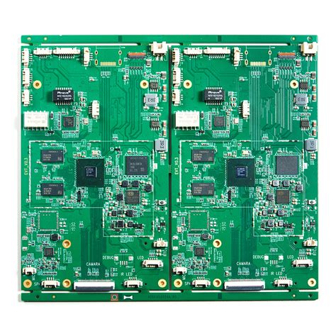
Material Selection for High-Speed PCB Via Performance
When designing high-speed printed circuit boards (PCBs), the selection of materials plays a crucial role in ensuring optimal via performance. Vias, which are the conductive pathways that connect different layers of a PCB, are integral to the board’s overall functionality, especially in high-speed applications where signal integrity is paramount. As electronic devices continue to evolve, demanding faster data transmission rates and higher frequencies, the importance of choosing the right materials for high-speed PCB vias cannot be overstated.
To begin with, the dielectric material used in the PCB substrate significantly impacts the performance of high-speed vias.
Dielectric materials with low loss tangents are preferred because they minimize signal attenuation and maintain signal integrity across the board. Materials such as polytetrafluoroethylene (PTFE) and certain ceramic-filled laminates are often chosen for their excellent electrical properties, including low dielectric constant and low dissipation factor. These characteristics help reduce signal loss and crosstalk, which are critical considerations in high-speed applications.
Moreover, the choice of copper for via plating is another essential factor.
Copper is widely used due to its excellent electrical conductivity and reliability. However, the thickness and quality of the copper plating can affect the via’s performance. Thicker copper layers can handle higher current loads, which is beneficial for power distribution in high-speed circuits. Additionally, ensuring that the copper plating is free from impurities and voids is vital to prevent signal degradation and potential failures.
Transitioning to the aspect of via design, the geometry and size of the via also influence its performance.
Smaller vias, often referred to as microvias, are increasingly used in high-speed PCBs due to their ability to reduce parasitic inductance and capacitance. This reduction is crucial for maintaining signal integrity at high frequencies. However, the material used must support the mechanical stability of these smaller vias to prevent issues such as cracking or delamination during thermal cycling.
Furthermore, the thermal properties of the materials used in high-speed PCBs are equally important.
High-speed circuits often generate significant heat, and the materials must be able to dissipate this heat effectively to prevent thermal-induced failures. Materials with high thermal conductivity, such as certain metal-filled laminates, can help manage heat dissipation. Additionally, the coefficient of thermal expansion (CTE) of the materials should be compatible with the components and solder used to avoid mechanical stress and potential damage during temperature fluctuations.
In addition to these considerations, the environmental stability of the materials is also a factor.
High-speed PCBs are often used in environments that may expose them to moisture, chemicals, and other harsh conditions. Therefore, selecting materials that offer resistance to these environmental factors is essential to ensure long-term reliability and performance.
In conclusion, the selection of materials for high-speed PCB vias is a multifaceted decision that requires careful consideration of electrical, thermal, mechanical, and environmental properties. By choosing materials that offer low dielectric loss, excellent thermal management, and robust mechanical stability, designers can enhance the performance and reliability of high-speed PCBs. As technology continues to advance, the demand for high-speed applications will only increase, making the careful selection of materials more critical than ever in achieving optimal via performance.
Thermal Management Strategies for High-Speed PCB Vias
In the realm of high-speed printed circuit boards (PCBs), the management of thermal energy is a critical consideration, particularly when it comes to the design and implementation of vias. These small, conductive pathways are essential for connecting different layers of a PCB, allowing signals to traverse the board efficiently. However, as the speed and complexity of electronic devices increase, so too does the heat generated by these components. Consequently, effective thermal management strategies for high-speed PCB vias are paramount to ensure both performance and reliability.
To begin with, it is important to understand the role of vias in high-speed PCBs.
Vias serve as vertical interconnections that facilitate the transmission of electrical signals between the various layers of a multilayer PCB. In high-speed applications, these vias must be designed to handle significant amounts of data at rapid speeds, which inherently generates heat. If not properly managed, this heat can lead to signal degradation, component failure, and reduced overall performance of the electronic device.
One of the primary strategies for managing thermal energy in high-speed PCB vias is through the use of thermal vias.
These are specialized vias designed specifically to dissipate heat away from critical components. By strategically placing thermal vias around heat-generating components, designers can create a more efficient thermal pathway, allowing heat to be conducted away from sensitive areas and dispersed throughout the board. This not only helps in maintaining optimal operating temperatures but also enhances the longevity and reliability of the PCB.
In addition to thermal vias, the choice of materials plays a significant role in thermal management.
High-speed PCBs often utilize materials with high thermal conductivity, such as copper, to facilitate better heat dissipation. Copper’s excellent thermal properties make it an ideal choice for both the vias and the surrounding traces, ensuring that heat is effectively spread across the board. Moreover, the use of advanced dielectric materials with low thermal resistance can further enhance the board’s ability to manage heat, providing a more stable environment for high-speed signal transmission.
Another effective approach involves optimizing the via design itself.
By adjusting the size, shape, and placement of vias, designers can influence the thermal performance of the PCB. For instance, increasing the diameter of a via can enhance its ability to conduct heat, while the use of via arrays can provide a more uniform distribution of thermal energy. Additionally, employing techniques such as back-drilling can reduce the parasitic capacitance and inductance associated with vias, thereby minimizing signal loss and improving overall thermal performance.
Furthermore, the integration of thermal management software tools during the design phase can provide valuable insights into the thermal behavior of high-speed PCB vias.
These tools allow designers to simulate various scenarios, assess potential thermal hotspots, and make informed decisions regarding via placement and board layout. By leveraging these advanced technologies, designers can optimize the thermal performance of their PCBs, ensuring that they meet the stringent demands of high-speed applications.
In conclusion, the management of thermal energy in high-speed PCB vias is a multifaceted challenge that requires a comprehensive approach. By employing strategies such as the use of thermal vias, selecting appropriate materials, optimizing via design, and utilizing thermal management software, designers can effectively mitigate the risks associated with excessive heat generation. As electronic devices continue to evolve and demand higher speeds, the importance of these thermal management strategies will only continue to grow, underscoring their critical role in the development of reliable and efficient high-speed PCBs.