High speed pcb stackup
Understanding High-Speed PCB Stackup Design Principles
In the realm of modern electronics, the design of high-speed printed circuit boards (PCBs) is a critical factor that influences the performance and reliability of electronic devices. As technology advances, the demand for faster data transmission and higher processing speeds necessitates a deeper understanding of high-speed PCB stackup design principles.
At the core of this design process is the stackup configuration, which plays a pivotal role in determining the electrical performance of the PCB.
By carefully considering the stackup, designers can mitigate issues such as signal integrity, electromagnetic interference, and power distribution, thereby enhancing the overall functionality of the device.
To begin with, the stackup of a high-speed PCB refers to the arrangement of conductive and insulating layers within the board.
This configuration is crucial because it directly affects the impedance control, crosstalk, and signal integrity of the PCB. In high-speed applications, maintaining consistent impedance is essential to ensure that signals propagate without distortion. Therefore, selecting the appropriate materials and layer thicknesses is vital to achieving the desired impedance levels. Typically, a high-speed PCB stackup consists of multiple layers, including signal layers, power planes, and ground planes. The strategic placement of these layers can significantly influence the board’s performance.
Moreover, the separation between signal layers and reference planes is a key consideration in high-speed PCB stackup design.
By minimizing the distance between these layers, designers can reduce the loop area, which in turn decreases the inductance and enhances signal integrity. Additionally, the use of ground planes adjacent to signal layers helps to provide a return path for high-frequency signals, thereby reducing electromagnetic interference. This configuration not only improves signal quality but also aids in the effective dissipation of heat, which is a common challenge in high-speed applications.
Transitioning to the topic of crosstalk, it is imperative to understand that the proximity of signal traces can lead to unwanted coupling, which adversely affects signal integrity.
To mitigate crosstalk, designers often employ techniques such as increasing the spacing between traces and using differential signaling. Differential pairs, which consist of two complementary signals, are particularly effective in high-speed designs as they offer improved noise immunity and reduced electromagnetic emissions. Furthermore, the careful routing of traces and the use of vias can help to minimize crosstalk and ensure optimal signal performance.
In addition to signal integrity, power distribution is another critical aspect of high-speed PCB stackup design.
A well-designed power distribution network (PDN) is essential to provide stable power to all components on the board. By incorporating dedicated power and ground planes, designers can achieve low impedance paths for power delivery, thereby reducing voltage fluctuations and ensuring reliable operation. The use of decoupling capacitors strategically placed near power pins further enhances the PDN by filtering out high-frequency noise.
In conclusion, understanding high-speed PCB stackup design principles is fundamental to the development of efficient and reliable electronic devices. By carefully considering factors such as impedance control, crosstalk mitigation, and power distribution, designers can optimize the performance of high-speed PCBs. As technology continues to evolve, the importance of mastering these design principles will only grow, underscoring the need for ongoing research and innovation in this field. Through meticulous planning and execution, high-speed PCB stackup design can pave the way for the next generation of electronic advancements.
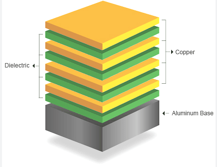
Key Materials for High-Speed PCB Stackup
In the realm of high-speed printed circuit board (PCB) design, the selection of materials for the stackup is a critical factor that significantly influences the performance, reliability, and manufacturability of the final product.
As electronic devices continue to evolve, demanding faster data rates and higher frequencies, the importance of choosing the right materials for high-speed PCB stackups cannot be overstated.
To begin with, the dielectric material is a fundamental component in the stackup, as it affects signal integrity, impedance control, and overall electrical performance.
Commonly used dielectric materials include FR-4, a glass-reinforced epoxy laminate, which is favored for its cost-effectiveness and versatility. However, for high-speed applications, materials with lower dielectric constants and dissipation factors, such as Rogers or Taconic laminates, are often preferred. These materials offer superior electrical properties, enabling better signal propagation and reduced signal loss.
Transitioning to the conductive layers, copper is the standard choice due to its excellent electrical conductivity and availability.
The thickness of the copper layers, often measured in ounces per square foot, plays a crucial role in determining the current-carrying capacity and thermal performance of the PCB. For high-speed applications, thinner copper layers are typically used to minimize skin effect losses, which become more pronounced at higher frequencies. Additionally, surface finishes such as immersion gold or silver are applied to the copper to enhance solderability and protect against oxidation, further ensuring reliable performance.
Moreover, the choice of prepreg materials, which are used to bond the layers of the PCB together, is another vital consideration.
Prepregs are impregnated with resin and serve as the adhesive between the core and copper layers. The resin content and glass weave style of the prepreg can impact the dielectric properties and mechanical stability of the PCB. For high-speed designs, low-loss prepregs with uniform glass weaves are preferred to maintain consistent impedance and reduce signal skew.
Furthermore, the solder mask, a protective layer applied over the copper traces, is essential for preventing short circuits and protecting the board from environmental factors.
In high-speed applications, the solder mask material should have a low dielectric constant to minimize its impact on signal integrity. Additionally, the color of the solder mask can influence the thermal performance of the PCB, with darker colors generally absorbing more heat.
In addition to these materials, the overall stackup configuration, including the number of layers and their arrangement, is crucial for optimizing signal integrity and minimizing electromagnetic interference (EMI). High-speed PCBs often employ multi-layer stackups with dedicated ground and power planes to provide a low-impedance path for return currents and to shield sensitive signals from external noise sources.
In conclusion, the selection of materials for high-speed PCB stackups is a complex process that requires careful consideration of electrical, thermal, and mechanical properties. By choosing the appropriate dielectric materials, copper thickness, prepregs, and solder masks, designers can achieve optimal performance and reliability in high-speed applications. As technology continues to advance, the demand for high-speed PCBs will only increase, making the understanding of key materials and their impact on PCB performance more important than ever.
Signal Integrity Challenges in High-Speed PCB Stackup
In the realm of modern electronics, the demand for high-speed performance has become a critical factor in the design and development of printed circuit boards (PCBs). As devices become more sophisticated, the need for efficient and reliable high-speed PCB stackups has grown exponentially. However, with this advancement comes a set of challenges, particularly concerning signal integrity. Signal integrity refers to the preservation of the quality of electrical signals as they travel through the PCB, and it is paramount in ensuring the proper functioning of high-speed circuits.
One of the primary challenges in maintaining signal integrity in high-speed PCB stackups is the issue of impedance control.
Impedance mismatches can lead to signal reflections, which degrade the quality of the signal and can cause data errors. To mitigate this, careful consideration must be given to the materials used in the PCB stackup, as well as the geometry of the traces. The dielectric constant of the substrate material, for instance, plays a crucial role in determining the impedance of the traces. By selecting materials with appropriate dielectric properties and designing trace geometries that match the desired impedance, designers can minimize reflections and maintain signal integrity.
Moreover, crosstalk is another significant concern in high-speed PCB stackups.
Crosstalk occurs when a signal in one trace induces an unwanted signal in an adjacent trace, leading to interference and potential data corruption. To address this, designers often employ techniques such as increasing the spacing between traces, using differential signaling, and incorporating ground planes to provide a return path for signals. These strategies help to isolate signals and reduce the likelihood of crosstalk, thereby preserving signal integrity.
In addition to impedance control and crosstalk, the issue of signal attenuation must also be considered.
As signals travel through the PCB, they can lose strength due to the resistive and dielectric losses inherent in the materials. This attenuation can be particularly problematic in high-speed applications, where even small losses can significantly impact performance. To combat this, designers may opt for low-loss materials and employ techniques such as via optimization to minimize signal degradation. By carefully managing these factors, it is possible to maintain signal strength and ensure reliable data transmission.
Furthermore, electromagnetic interference (EMI) poses a challenge to signal integrity in high-speed PCB stackups.
EMI can originate from both internal and external sources, and it can disrupt the operation of sensitive circuits. To mitigate EMI, designers often implement shielding techniques, such as using ground planes and incorporating decoupling capacitors, to suppress unwanted noise. Additionally, proper layout practices, such as minimizing loop areas and ensuring adequate separation between high-speed and low-speed signals, can help reduce the impact of EMI on signal integrity.
In conclusion, maintaining signal integrity in high-speed PCB stackups is a multifaceted challenge that requires careful consideration of various factors. By addressing issues such as impedance control, crosstalk, signal attenuation, and electromagnetic interference, designers can create PCB stackups that support high-speed performance while ensuring reliable operation. As technology continues to advance, the importance of signal integrity in high-speed applications will only grow, making it an essential consideration for engineers and designers in the field. Through meticulous design and innovative solutions, the challenges of signal integrity in high-speed PCB stackups can be effectively managed, paving the way for the next generation of electronic devices.
Best Practices for Layer Arrangement in High-Speed PCB Stackup
In the realm of high-speed printed circuit board (PCB) design, the arrangement of layers within the stackup is a critical factor that can significantly influence the performance and reliability of the final product. As electronic devices continue to demand faster processing speeds and greater functionality, the need for meticulous attention to PCB stackup design becomes increasingly paramount. To achieve optimal performance, designers must consider several best practices when arranging layers in a high-speed PCB stackup.
To begin with, understanding the fundamental purpose of each layer is essential.
Typically, a high-speed PCB stackup consists of signal layers, power planes, and ground planes. Signal layers are responsible for carrying data and control signals, while power and ground planes provide stable voltage references and return paths for signals. The strategic placement of these layers can mitigate issues such as electromagnetic interference (EMI) and signal integrity problems, which are common in high-speed applications.
One of the primary considerations in layer arrangement is the minimization of loop areas.
By placing power and ground planes adjacent to each other, designers can create a low-inductance path that reduces the loop area for return currents. This configuration not only enhances signal integrity but also minimizes EMI, as smaller loop areas are less susceptible to radiating unwanted electromagnetic noise. Furthermore, it is advisable to position high-speed signal layers between two ground planes, forming a microstrip or stripline configuration. This arrangement provides controlled impedance and reduces crosstalk between adjacent signal traces.
In addition to minimizing loop areas, maintaining consistent impedance throughout the PCB is crucial.
Impedance mismatches can lead to signal reflections, which degrade signal quality and can cause data errors. To achieve consistent impedance, designers should carefully select the dielectric materials and thicknesses between layers. Moreover, ensuring uniform trace widths and spacing on signal layers is vital for maintaining the desired impedance levels. By adhering to these practices, designers can enhance signal integrity and ensure reliable data transmission.
Another important aspect of high-speed PCB stackup design is the separation of analog and digital signals.
Mixing these signals on the same layer can lead to interference and signal degradation. Therefore, it is recommended to allocate separate layers for analog and digital signals, or at the very least, to maintain sufficient spacing between them. This separation helps to preserve signal quality and prevents unwanted interactions between different types of signals.
Thermal management is also a key consideration in high-speed PCB design.
As electronic components operate at higher speeds, they generate more heat, which can affect performance and reliability. To address this, designers should incorporate thermal vias and copper pours to facilitate heat dissipation. Additionally, placing power and ground planes closer to heat-generating components can help distribute heat more evenly across the PCB.
Finally, collaboration with fabrication partners is essential to ensure that the stackup design is manufacturable and cost-effective.
Engaging with manufacturers early in the design process allows for valuable feedback on material selection, layer count, and other factors that can impact production. By working closely with fabrication partners, designers can optimize the stackup for both performance and manufacturability.
In conclusion, the arrangement of layers in a high-speed PCB stackup is a complex but crucial aspect of modern electronic design. By minimizing loop areas, maintaining consistent impedance, separating analog and digital signals, managing thermal considerations, and collaborating with fabrication partners, designers can create high-performance PCBs that meet the demands of today’s advanced electronic applications.