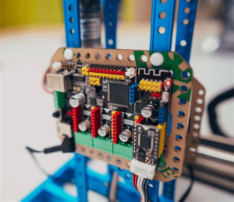
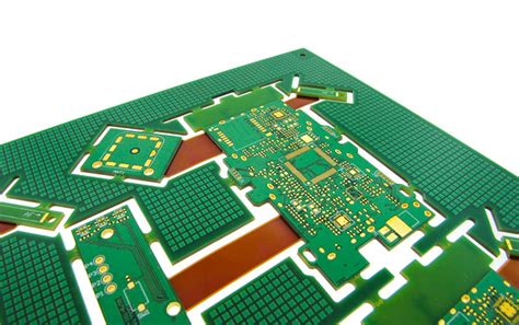
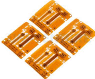
High speed pcb routing guidelines
Importance Of Signal Integrity In High Speed PCB Routing guidelines
In the realm of high-speed printed circuit board (PCB) design, signal integrity emerges as a critical factor that can significantly influence the performance and reliability of electronic systems.
As technology advances, the demand for faster data transmission rates and higher processing speeds continues to grow, necessitating meticulous attention to signal integrity during the PCB routing process. Ensuring signal integrity in high-speed PCB routing is paramount, as it directly impacts the functionality and efficiency of the entire electronic system.
Signal integrity refers to the preservation of the quality and fidelity of electrical signals as they traverse through the PCB.
In high-speed applications, signals are susceptible to various forms of degradation, including reflections, crosstalk, and electromagnetic interference (EMI). These issues can lead to signal distortion, data corruption, and ultimately, system failure. Therefore, understanding and mitigating these challenges is essential for engineers and designers working on high-speed PCBs.
One of the primary concerns in high-speed PCB routing is the management of reflections.
Reflections occur when a signal encounters an impedance discontinuity along its transmission path, causing a portion of the signal to be reflected back towards the source. This can result in signal degradation and timing errors. To minimize reflections, it is crucial to maintain consistent impedance throughout the signal path. This can be achieved by carefully controlling trace widths, spacing, and the dielectric properties of the PCB material. Additionally, employing proper termination techniques, such as series or parallel termination, can help absorb reflected signals and maintain signal integrity.
Crosstalk is another significant issue that can compromise signal integrity in high-speed PCB routing.
Crosstalk occurs when a signal on one trace induces unwanted noise on an adjacent trace, leading to interference and potential data errors. To mitigate crosstalk, designers should ensure adequate spacing between traces and utilize ground planes to provide effective shielding. Furthermore, routing high-speed signals on different layers and using differential pairs can help reduce crosstalk by minimizing the coupling between adjacent traces.
Electromagnetic interference (EMI) poses yet another challenge to signal integrity in high-speed PCB routing.
EMI can originate from both internal and external sources, disrupting the normal operation of electronic components. To combat EMI, designers should implement proper grounding techniques, such as using a solid ground plane and ensuring low-inductance connections. Additionally, incorporating decoupling capacitors near power pins can help filter out high-frequency noise and stabilize power delivery.
Transitioning from these technical considerations, it is also important to emphasize the role of simulation and analysis tools in maintaining signal integrity.
Advanced simulation software allows designers to model and predict the behavior of high-speed signals, enabling them to identify potential issues and optimize the PCB layout before fabrication. By leveraging these tools, engineers can make informed decisions regarding trace routing, layer stack-up, and component placement, ultimately enhancing signal integrity.
In conclusion, the importance of signal integrity in high-speed PCB routing cannot be overstated. As electronic systems continue to evolve, maintaining signal integrity becomes increasingly challenging yet essential. By addressing issues such as reflections, crosstalk, and EMI, and utilizing simulation tools, designers can ensure that high-speed PCBs deliver optimal performance and reliability. Consequently, a thorough understanding of signal integrity principles and best practices is indispensable for engineers striving to meet the demands of modern high-speed electronic applications.
Best Practices For Layer Stackup In High-Speed PCB Design
In the realm of high-speed PCB design, the layer stackup plays a pivotal role in ensuring signal integrity, minimizing electromagnetic interference, and optimizing overall performance. As electronic devices become increasingly complex, the demand for efficient and reliable high-speed circuits has surged, making it imperative for designers to adhere to best practices in layer stackup configuration. A well-considered layer stackup not only enhances the electrical performance of a PCB but also contributes to its manufacturability and cost-effectiveness.
To begin with, understanding the fundamental principles of layer stackup is crucial.
A typical high-speed PCB consists of multiple layers, each serving a specific purpose. These layers generally include signal layers, power planes, and ground planes. The arrangement and number of these layers are determined by the design requirements, such as signal speed, impedance control, and thermal management. A balanced stackup, where the layers are symmetrically arranged around the center of the PCB, is often recommended to prevent warping during the manufacturing process.
One of the primary considerations in high-speed PCB layer stackup is impedance control.
Impedance mismatches can lead to signal reflections, which degrade signal quality and can cause data errors. To achieve controlled impedance, designers must carefully select the dielectric materials and thicknesses between layers. The use of high-quality, low-loss dielectric materials is advisable, as they help maintain signal integrity at high frequencies. Additionally, maintaining consistent trace widths and spacing is essential to ensure uniform impedance across the board.
Another critical aspect is the separation of signal layers by ground or power planes.
This practice helps in reducing crosstalk between adjacent signal traces, which is particularly important in high-speed designs where signals can couple and interfere with each other. By placing a ground plane between two signal layers, designers can create a microstrip or stripline configuration, which provides a controlled impedance environment and minimizes electromagnetic interference.
Thermal management is also a significant consideration in high-speed PCB design.
As the speed and density of electronic components increase, so does the heat generated by the PCB. A well-designed layer stackup can aid in effective heat dissipation. Incorporating dedicated thermal vias and using thicker copper layers for power and ground planes can help distribute heat more evenly across the board, preventing hotspots and ensuring reliable operation.
Furthermore, the choice of via technology can impact the performance of high-speed PCBs.
Blind and buried vias are often used in high-density designs to connect different layers without occupying valuable surface space. However, these vias can introduce parasitic inductance and capacitance, which may affect signal integrity. Therefore, careful consideration of via placement and size is necessary to minimize their impact on high-speed signals.
In conclusion, the layer stackup in high-speed PCB design is a critical factor that influences the electrical performance, manufacturability, and cost of the final product. By adhering to best practices such as impedance control, strategic layer arrangement, effective thermal management, and judicious via selection, designers can create PCBs that meet the demanding requirements of modern high-speed applications. As technology continues to evolve, staying informed about the latest materials and techniques will be essential for achieving optimal results in high-speed PCB design.
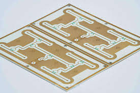
Techniques For Minimizing Crosstalk In High-Speed PCB Layouts
In the realm of high-speed printed circuit board (PCB) design, minimizing crosstalk is a critical consideration to ensure signal integrity and optimal performance. Crosstalk, the unwanted coupling of signals between adjacent traces, can lead to data corruption and degraded system performance, particularly in high-speed applications. Therefore, understanding and implementing effective techniques to mitigate crosstalk is essential for engineers and designers working in this field.
To begin with, one of the fundamental strategies for minimizing crosstalk is to maintain adequate spacing between signal traces.
By increasing the distance between adjacent traces, the electromagnetic interference that causes crosstalk is significantly reduced. This approach is particularly effective in high-speed designs where signal integrity is paramount. Additionally, employing differential signaling can further mitigate crosstalk. Differential pairs, which consist of two complementary signals, are less susceptible to external noise and crosstalk because the interference affects both signals equally, allowing the receiver to cancel out the noise.
Moreover, the use of ground planes is another effective technique in reducing crosstalk.
Ground planes act as a shield, providing a return path for the signals and minimizing the loop area, which in turn reduces the inductive coupling between traces. It is advisable to place a continuous ground plane adjacent to the signal layer to enhance this effect. Furthermore, ensuring that the ground plane is unbroken and free of slots or gaps is crucial, as discontinuities can exacerbate crosstalk issues.
In addition to spacing and grounding strategies, careful consideration of trace routing is vital.
Routing traces orthogonally on adjacent layers can help minimize crosstalk by reducing the parallel coupling length between traces. This technique, known as orthogonal routing, is particularly beneficial in multi-layer PCBs where space constraints often necessitate close trace proximity. Additionally, avoiding long parallel runs of traces and using serpentine routing for delay matching can further reduce the potential for crosstalk.
Another important aspect to consider is the impedance control of traces.
Maintaining consistent impedance along the length of a trace helps prevent reflections and signal integrity issues that can contribute to crosstalk. This can be achieved by carefully designing the trace width, spacing, and dielectric material properties to match the desired impedance. Furthermore, using controlled impedance traces in conjunction with proper termination techniques can significantly enhance signal integrity and reduce crosstalk.
Moreover, the implementation of guard traces, also known as shielding traces, can be an effective method for crosstalk reduction.
Guard traces are placed between critical signal traces and connected to the ground plane at regular intervals. These traces act as a barrier, absorbing and redirecting the electromagnetic interference away from the signal traces. However, it is important to ensure that guard traces are properly terminated to prevent them from becoming a source of crosstalk themselves.
In conclusion, minimizing crosstalk in high-speed PCB layouts requires a comprehensive approach that encompasses trace spacing, grounding, routing, impedance control, and the use of guard traces. By carefully considering these factors and implementing appropriate design techniques, engineers can significantly enhance the performance and reliability of high-speed PCBs. As technology continues to advance and the demand for faster data rates increases, the importance of effective crosstalk mitigation strategies will only grow, making it an essential area of focus for PCB designers.
Effective Use Of Ground Planes In High-Speed PCB Routing
In the realm of high-speed printed circuit board (PCB) design, the effective use of ground planes is paramount to ensuring signal integrity and minimizing electromagnetic interference (EMI). As electronic devices become increasingly complex and operate at higher frequencies, the challenges associated with high-speed PCB routing have intensified. Ground planes, when utilized correctly, can significantly mitigate these challenges by providing a low-impedance path for return currents and reducing the potential for signal distortion.
To begin with, it is essential to understand the role of ground planes in high-speed PCB design.
Ground planes serve as a reference point for all signals on the board, offering a stable voltage level against which other voltages are measured. This stability is crucial for maintaining signal integrity, particularly in high-speed applications where even minor voltage fluctuations can lead to data errors. Moreover, ground planes help in reducing the loop area of signal paths, thereby minimizing inductance and the associated EMI.
Incorporating ground planes effectively requires careful consideration of their placement and connectivity.
Ideally, a continuous ground plane should be placed directly beneath the signal layers. This configuration not only provides a consistent return path for signals but also helps in shielding sensitive traces from external noise. When designing multilayer PCBs, it is advisable to dedicate at least one entire layer to the ground plane. This approach ensures that the ground plane is uninterrupted, which is critical for maintaining a low-impedance path.
Furthermore, the concept of return path continuity is vital in high-speed PCB routing.
As signals traverse the board, they generate return currents that naturally seek the path of least impedance. If the ground plane is fragmented or contains slots, these return currents may be forced to take longer paths, increasing the loop area and, consequently, the inductance. This can lead to increased EMI and potential signal integrity issues. Therefore, maintaining a continuous ground plane without unnecessary splits or gaps is crucial.
In addition to continuity, the proximity of the ground plane to the signal traces is another important factor.
The closer the ground plane is to the signal layer, the better the coupling between the signal and its return path. This close coupling reduces the loop area and enhances the board’s ability to suppress EMI. Designers should aim to minimize the dielectric thickness between the signal layer and the ground plane to achieve this effect.
Moreover, stitching vias play a significant role in maintaining ground plane integrity across different layers.
These vias connect ground planes on multiple layers, ensuring that return paths remain consistent throughout the board. Proper placement of stitching vias is essential, particularly near high-speed signal transitions and around the periphery of the board, to prevent the formation of large loop areas.
In conclusion, the effective use of ground planes in high-speed PCB routing is a critical aspect of modern electronic design. By ensuring continuous, closely coupled ground planes and strategically placing stitching vias, designers can significantly enhance signal integrity and reduce EMI. As technology continues to advance, the principles of effective ground plane utilization will remain a cornerstone of successful high-speed PCB design, enabling the development of faster, more reliable electronic devices.