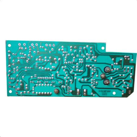
High speed pcb traces
Importance Of Impedance Control In High-Speed PCB Traces
In the realm of high-speed printed circuit board (PCB) design, the significance of impedance control cannot be overstated. As electronic devices continue to evolve, demanding faster processing speeds and higher data rates, the need for precise impedance control in PCB traces becomes increasingly critical.
Impedance, in the context of PCB traces, refers to the resistance that an electrical signal encounters as it travels along the trace.
This resistance is not merely a function of the trace’s material but is also influenced by its geometry, the dielectric material of the PCB, and the frequency of the signal.
Therefore, understanding and controlling impedance is essential for ensuring signal integrity and minimizing potential issues such as signal reflection, crosstalk, and electromagnetic interference.
To begin with, signal integrity is a paramount concern in high-speed PCB design.
When signals travel at high speeds, any impedance mismatch along the trace can lead to reflections. These reflections can cause signal distortion, leading to data errors and degraded performance.
By maintaining consistent impedance along the trace, designers can minimize these reflections, thereby preserving the integrity of the signal. This is particularly important in applications such as telecommunications, computing, and consumer electronics, where even minor signal degradation can have significant consequences.
Moreover, impedance control is crucial for reducing crosstalk, which occurs when a signal in one trace induces an unwanted signal in an adjacent trace.
In high-speed designs, traces are often placed in close proximity to one another to save space and reduce the overall size of the PCB. However, this proximity increases the risk of crosstalk, which can lead to data corruption and system instability. By carefully controlling the impedance of each trace, designers can mitigate the effects of crosstalk, ensuring that signals remain isolated and free from interference.
In addition to signal integrity and crosstalk, electromagnetic interference (EMI) is another challenge that can be addressed through impedance control.
High-speed signals can generate electromagnetic fields that interfere with other components on the PCB or with external devices. This interference can disrupt the operation of the device and lead to compliance issues with regulatory standards. By designing traces with controlled impedance, designers can minimize the generation of electromagnetic fields, thereby reducing the potential for EMI.
Furthermore, achieving precise impedance control requires a comprehensive understanding of the materials and processes involved in PCB fabrication.
The choice of dielectric material, for instance, plays a significant role in determining the impedance of a trace.
Materials with different dielectric constants will affect the capacitance and inductance of the trace, thereby influencing its impedance. Additionally, the trace width, thickness, and spacing must be carefully calculated to achieve the desired impedance.
Advanced simulation tools and software are often employed to model and predict the impedance of traces before fabrication, allowing designers to make informed decisions and adjustments.
In conclusion, the importance of impedance control in high-speed PCB traces cannot be underestimated.
As electronic devices continue to push the boundaries of speed and performance, ensuring signal integrity, minimizing crosstalk, and reducing electromagnetic interference become critical design considerations. By understanding and controlling the factors that influence impedance, designers can create PCBs that meet the demanding requirements of modern high-speed applications, ultimately leading to more reliable and efficient electronic devices.
Techniques For Minimizing Signal Loss In High-Speed PCB Design
In the realm of high-speed printed circuit board (PCB) design, minimizing signal loss is a critical concern that demands meticulous attention to detail. As electronic devices continue to evolve, the need for faster data transmission rates has become paramount, necessitating the development of techniques that ensure signal integrity. One of the primary challenges in high-speed PCB design is the attenuation of signals as they traverse the traces, which can lead to data corruption and system malfunctions. Therefore, understanding and implementing effective strategies to mitigate signal loss is essential for engineers and designers.
To begin with, the choice of materials plays a significant role in minimizing signal loss.
High-frequency signals are particularly susceptible to dielectric losses, which occur when the insulating material between the conductive layers absorbs energy. Selecting materials with low dielectric constants and low loss tangents can significantly reduce these losses. For instance, using advanced laminates such as polytetrafluoroethylene (PTFE) or specialized low-loss FR-4 variants can enhance signal integrity by minimizing dielectric absorption.
Moreover, the geometry of the PCB traces is another crucial factor.
The width and thickness of the traces, as well as the spacing between them, can influence the impedance and, consequently, the signal quality. To maintain consistent impedance and reduce reflections, it is advisable to use controlled impedance traces. This involves carefully calculating the trace dimensions and the dielectric properties of the substrate to match the characteristic impedance of the transmission line. By doing so, designers can ensure that the signal travels with minimal distortion and reflection.
In addition to material selection and trace geometry, the layout of the PCB is instrumental in minimizing signal loss.
High-speed signals are prone to electromagnetic interference (EMI) and crosstalk, which can degrade signal quality. To mitigate these effects, it is essential to implement proper grounding techniques and maintain adequate separation between high-speed traces. Utilizing ground planes and ensuring that signal return paths are short and direct can help reduce EMI. Furthermore, employing differential signaling, where two complementary signals are transmitted simultaneously, can effectively cancel out noise and improve signal integrity.
Another technique to consider is the use of vias, which are vertical connections between different layers of a PCB.
While vias are necessary for multi-layer boards, they can introduce signal loss due to parasitic inductance and capacitance. To minimize these effects, it is advisable to use blind or buried vias, which do not pass through all layers, thereby reducing the associated parasitic elements. Additionally, minimizing the number of vias in high-speed signal paths can further enhance signal integrity.
Finally, simulation and testing are indispensable in the design process.
Advanced simulation tools allow designers to model and analyze the behavior of high-speed signals on a PCB, enabling them to identify potential issues and optimize the design before fabrication.
Post-fabrication testing, such as time-domain reflectometry (TDR) and vector network analysis, can provide valuable insights into the actual performance of the PCB, allowing for further refinements if necessary.
In conclusion, minimizing signal loss in high-speed PCB design requires a comprehensive approach that encompasses material selection, trace geometry, layout considerations, and thorough testing. By employing these techniques, designers can ensure that their PCBs meet the demanding requirements of modern electronic devices, thereby enhancing performance and reliability. As technology continues to advance, the importance of mastering these techniques will only grow, underscoring the need for ongoing innovation and expertise in the field of high-speed PCB design.
Best Practices For Routing High-Speed PCB Traces
Routing high-speed PCB traces is a critical aspect of modern electronic design, as it directly influences the performance and reliability of electronic devices. As technology advances, the demand for faster data transmission and higher processing speeds necessitates meticulous attention to detail in PCB design. To achieve optimal performance, several best practices should be adhered to when routing high-speed PCB traces.
Firstly, it is essential to understand the significance of impedance control in high-speed PCB design.
Impedance mismatches can lead to signal reflections, which degrade signal integrity and can cause data errors. To mitigate this, designers should ensure that traces are routed with consistent width and spacing, maintaining a uniform impedance throughout the trace. Utilizing controlled impedance traces, often achieved through microstrip or stripline configurations, can help maintain signal integrity by minimizing reflections and ensuring that signals propagate smoothly.
In addition to impedance control, minimizing crosstalk is crucial in high-speed PCB design.
Crosstalk occurs when signals on adjacent traces interfere with each other, leading to potential data corruption. To reduce crosstalk, designers should maintain adequate spacing between high-speed traces and consider using ground planes or guard traces to isolate them. Furthermore, routing high-speed traces on different layers can help minimize the risk of crosstalk by providing additional separation between signals.
Another important consideration is the management of signal return paths.
High-speed signals require a low-impedance return path to prevent signal distortion and maintain signal integrity. Ensuring that return paths are as short and direct as possible is vital. This can be achieved by placing ground planes directly beneath signal layers and avoiding breaks in the ground plane that could disrupt the return path. Additionally, using vias sparingly and strategically can help maintain a continuous return path, as excessive via usage can introduce inductance and disrupt signal flow.
Moreover, attention should be paid to trace length matching, especially in differential pairs.
Differential signaling is commonly used in high-speed designs due to its noise immunity and ability to maintain signal integrity over long distances. However, for differential pairs to function effectively, the traces must be of equal length to ensure that signals arrive simultaneously at the receiver. Length matching can be achieved through careful routing and the use of serpentine traces if necessary.
Transitioning to the topic of power integrity, it is imperative to ensure that power delivery networks (PDNs) are designed to support high-speed operation.
A well-designed PDN minimizes voltage fluctuations and provides stable power to all components. This can be accomplished by using decoupling capacitors strategically placed near power pins and ensuring that power and ground planes are adequately sized to handle the current demands of the circuit.
Finally, simulation and testing play a crucial role in validating high-speed PCB designs.
Utilizing simulation tools to model signal integrity, crosstalk, and power integrity can help identify potential issues before physical prototyping. Once the PCB is fabricated, thorough testing should be conducted to verify that the design meets performance specifications and operates reliably under real-world conditions.
In conclusion, routing high-speed PCB traces requires a comprehensive understanding of various factors that influence signal integrity and performance. By adhering to best practices such as impedance control, crosstalk minimization, proper signal return path management, trace length matching, and robust power integrity design, engineers can ensure that their high-speed PCBs deliver optimal performance and reliability. Through careful planning, simulation, and testing, designers can overcome the challenges associated with high-speed PCB design and meet the ever-increasing demands of modern electronic applications.

Impact Of Dielectric Materials On High-Speed PCB Performance
In the realm of high-speed printed circuit board (PCB) design, the choice of dielectric materials plays a pivotal role in determining the overall performance and reliability of the circuit. As electronic devices continue to evolve, demanding faster processing speeds and higher data rates, the significance of selecting appropriate dielectric materials becomes increasingly pronounced. Understanding the impact of these materials on high-speed PCB performance is essential for engineers and designers striving to optimize their designs for maximum efficiency and functionality.
To begin with, dielectric materials are integral to the construction of PCBs, serving as the insulating layer between conductive traces.
These materials influence several key electrical properties, including signal integrity, impedance control, and electromagnetic interference (EMI) mitigation. As signal frequencies increase, the dielectric constant (Dk) and dissipation factor (Df) of the material become critical parameters. A lower dielectric constant is generally preferred for high-speed applications, as it reduces signal propagation delay and minimizes signal distortion. Consequently, selecting a dielectric material with an appropriate Dk value is crucial for maintaining signal integrity and ensuring that high-speed signals are transmitted accurately across the PCB.
Moreover, the dissipation factor, which measures the dielectric material’s inherent energy loss, is another vital consideration.
A lower dissipation factor indicates that the material can efficiently transmit high-frequency signals with minimal energy loss, thereby preserving signal strength and reducing the risk of data errors. This is particularly important in high-speed applications where even minor signal degradation can lead to significant performance issues. Therefore, choosing a dielectric material with a low dissipation factor is essential for optimizing high-speed PCB performance.
In addition to electrical properties, thermal management is another aspect where dielectric materials exert a considerable impact.
High-speed PCBs often generate substantial heat due to increased power consumption and densely packed components. Dielectric materials with high thermal conductivity can effectively dissipate heat, preventing overheating and ensuring the longevity and reliability of the PCB. Consequently, selecting materials that offer a balance between electrical performance and thermal management is crucial for high-speed applications.
Furthermore, the mechanical properties of dielectric materials, such as their ability to withstand environmental stress and mechanical deformation, also influence high-speed PCB performance. Materials that exhibit high dimensional stability and resistance to thermal expansion are preferred, as they maintain their structural integrity under varying operating conditions. This stability is essential for preserving the alignment and spacing of high-speed traces, which is critical for maintaining signal integrity and preventing crosstalk.
As the demand for high-speed electronic devices continues to grow, advancements in dielectric materials are expected to play a significant role in shaping the future of PCB design.
Innovations in material science are likely to yield new dielectric materials with enhanced electrical, thermal, and mechanical properties, further pushing the boundaries of high-speed PCB performance. In conclusion, the impact of dielectric materials on high-speed PCB performance is multifaceted, encompassing electrical, thermal, and mechanical considerations. By carefully selecting materials that meet the specific requirements of high-speed applications, engineers and designers can ensure optimal performance, reliability, and longevity of their PCBs, ultimately contributing to the advancement of modern electronic technologies.