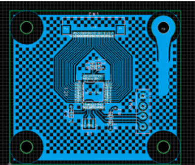
High speed pcb CAD
High Speed PCB CAD: Designing for the Future
Printed Circuit Boards (PCBs) are the backbone of modern electronic devices, and as technology advances, the demand for high-speed PCBs has grown exponentially. High-speed PCB design is a specialized field that requires a deep understanding of both electrical engineering principles and the capabilities of Computer-Aided Design (CAD) tools. This article explores the intricacies of high-speed PCB CAD, offering insights into its importance, challenges, and best practices.

Understanding High-Speed PCB Design
High-speed PCB design refers to the creation of circuit boards that can handle high-frequency signals and fast data rates. These designs are crucial for applications such as telecommunications, computing, and consumer electronics, where performance and reliability are paramount.
Key Characteristics of High-Speed PCBs
- Signal Integrity: Ensuring that signals are transmitted without distortion or loss.
- Power Integrity: Maintaining stable power delivery across the board.
- Thermal Management: Efficiently dissipating heat to prevent component failure.
- Electromagnetic Compatibility (EMC): Minimizing electromagnetic interference (EMI) and ensuring compliance with regulatory standards.
The Role of CAD in High-Speed PCB Design
Computer-Aided Design (CAD) tools are essential for designing high-speed PCBs. They provide engineers with the ability to simulate, analyze, and optimize their designs before physical prototyping.

Benefits of Using CAD Tools
- Precision and Accuracy: CAD tools offer precise control over component placement and routing.
- Simulation Capabilities: Engineers can simulate signal integrity, power integrity, and thermal performance.
- Design Rule Checks (DRC): Automated checks ensure compliance with design specifications and industry standards.
- Collaboration: CAD tools facilitate collaboration among design teams, allowing for seamless integration of different design aspects.
Challenges in High-Speed PCB Design
Designing high-speed PCBs presents several challenges that engineers must overcome to ensure optimal performance.
Signal Integrity Issues
Signal integrity is a critical concern in high-speed PCB design. Issues such as signal reflection, crosstalk, and impedance mismatches can degrade performance.
- Reflection: Occurs when signals encounter impedance discontinuities, leading to signal distortion.
- Crosstalk: Unwanted coupling between adjacent traces can cause interference.
- Impedance Mismatch: Variations in trace impedance can lead to signal loss and distortion.
Power Integrity Challenges
Power integrity involves ensuring that all components receive stable and sufficient power.
- Voltage Drops: Caused by resistance in power delivery networks, leading to insufficient power supply.
- Ground Bounce: Variations in ground potential can affect signal integrity.
- Decoupling: Proper placement of decoupling capacitors is essential to minimize voltage fluctuations.
Thermal Management
High-speed PCBs generate significant heat, which must be managed to prevent component failure.
- Heat Dissipation: Effective use of heat sinks, thermal vias, and copper pours is crucial.
- Material Selection: Choosing materials with high thermal conductivity can improve heat dissipation.
Best Practices for High-Speed PCB Design
To address the challenges of high-speed PCB design, engineers can adopt several best practices.
Design for Signal Integrity
- Controlled Impedance: Use controlled impedance traces to minimize signal reflection.
- Differential Pair Routing: Employ differential pairs for high-speed signals to reduce crosstalk.
- Short Trace Lengths: Keep trace lengths as short as possible to minimize signal delay.
Enhance Power Integrity
- Power Plane Design: Use dedicated power planes to reduce voltage drops and ground bounce.
- Decoupling Strategy: Place decoupling capacitors close to power pins to stabilize voltage.
- Via Optimization: Minimize the number of vias in power delivery paths to reduce inductance.
Optimize Thermal Management
- Thermal Vias: Use thermal vias to transfer heat from components to heat sinks.
- Copper Pours: Utilize copper pours to spread heat across the board.
- Component Placement: Arrange components to facilitate airflow and heat dissipation.
Case Studies in High-Speed PCB Design
Examining real-world examples can provide valuable insights into the application of high-speed PCB design principles.
Case Study 1: Telecommunications Equipment
A leading telecommunications company faced challenges with signal integrity in their high-speed routers. By implementing controlled impedance traces and differential pair routing, they achieved a 30% reduction in signal distortion, enhancing data transmission reliability.
Case Study 2: Consumer Electronics
A consumer electronics manufacturer needed to improve the thermal performance of their high-speed gaming consoles. By optimizing thermal vias and copper pours, they reduced operating temperatures by 15%, increasing device longevity and performance.
The Future of High-Speed PCB CAD
As technology continues to evolve, the demand for high-speed PCBs will only increase. Emerging trends such as 5G, the Internet of Things (IoT), and artificial intelligence (AI) will drive the need for even more sophisticated designs.
Emerging Technologies
- 5G Networks: Require PCBs capable of handling higher frequencies and data rates.
- IoT Devices: Demand compact, high-performance PCBs for seamless connectivity.
- AI Applications: Need advanced PCBs to support complex computations and data processing.
Advancements in CAD Tools
CAD tools are continually evolving to meet the demands of high-speed PCB design.
- AI-Driven Design: AI algorithms can optimize component placement and routing for improved performance.
- Cloud-Based Collaboration: Enables real-time collaboration among global design teams.
- Enhanced Simulation: Advanced simulation capabilities allow for more accurate predictions of PCB performance.
Optimizing Signal Integrity in High-Speed PCB CAD Design
In the realm of high-speed printed circuit board (PCB) design, optimizing signal integrity is paramount to ensuring the reliable performance of electronic devices. As technology advances, the demand for faster data transmission rates has increased, necessitating meticulous attention to the intricacies of PCB design. High-speed PCB computer-aided design (CAD) tools have become indispensable in addressing these challenges, offering designers the ability to simulate, analyze, and refine their designs to achieve optimal signal integrity.
Signal integrity refers to the preservation of the quality of electrical signals as they travel through a PCB.
In high-speed applications, signals are susceptible to various forms of degradation, including reflection, crosstalk, and electromagnetic interference. These issues can lead to data corruption, increased error rates, and ultimately, device malfunction. Therefore, understanding and mitigating these effects is crucial for designers working with high-speed PCBs.
One of the primary considerations in optimizing signal integrity is the careful management of impedance. Impedance mismatches can cause signal reflections, which degrade signal quality. High-speed PCB CAD tools allow designers to model and simulate the impedance of traces, vias, and other components, enabling them to make informed decisions about trace width, spacing, and layer stack-up. By ensuring that the impedance is consistent throughout the signal path, designers can minimize reflections and maintain signal integrity.
Conclusion
High-speed PCB design is a complex but essential aspect of modern electronics. By leveraging advanced CAD tools and adhering to best practices, engineers can overcome the challenges of signal integrity, power integrity, and thermal management. As technology advances, the role of high-speed PCB CAD will become increasingly critical in driving innovation across various industries.
In summary, high-speed PCB CAD is not just about designing faster circuits; it’s about ensuring reliability, efficiency, and performance in an ever-evolving technological landscape. By staying informed about the latest trends and tools, engineers can continue to push the boundaries of what’s possible in electronic design.