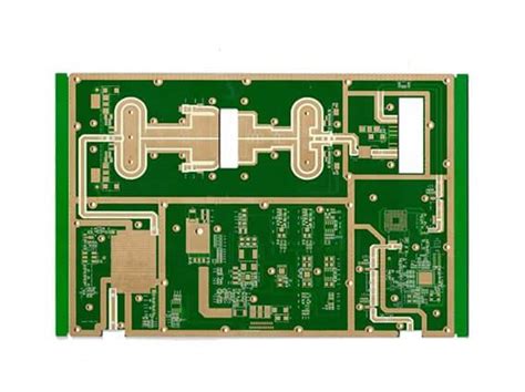
High frequency pcb board manufacturing
Understanding The Basics Of High Frequency PCB Design
High frequency PCB (Printed Circuit Board) design is a critical aspect of modern electronics, particularly in applications that require rapid signal transmission and minimal signal loss.
As technology advances, the demand for high frequency PCBs has surged, driven by the proliferation of wireless communication devices, advanced radar systems, and high-speed computing.
Understanding the basics of high frequency PCB design is essential for engineers and designers who aim to optimize performance and ensure reliability in these sophisticated applications.
To begin with, high frequency PCBs are designed to handle signals in the gigahertz range, which necessitates a meticulous approach to design and material selection.
The choice of substrate material is paramount, as it directly influences the board’s ability to manage high-speed signals. Materials such as PTFE (Polytetrafluoroethylene), ceramic-filled laminates, and other low-loss dielectric materials are commonly used due to their excellent electrical properties. These materials help minimize signal attenuation and maintain signal integrity, which are crucial for high frequency applications.
Moreover, the layout of a high frequency PCB is another critical factor that impacts its performance.
Signal integrity can be compromised by factors such as impedance mismatches, crosstalk, and electromagnetic interference (EMI). To mitigate these issues, designers must carefully consider trace width, spacing, and the overall stack-up of the PCB.
Controlled impedance is often required, which involves precise calculations and simulations to ensure that the traces can carry high frequency signals without distortion. Additionally, the use of ground planes and proper shielding techniques can significantly reduce EMI and crosstalk, further enhancing the board’s performance.
Transitioning to the manufacturing process, high frequency PCB fabrication demands a high level of precision and expertise.
The manufacturing process must accommodate the unique properties of the chosen materials, which often require specialized equipment and techniques. For instance, PTFE-based materials can be challenging to drill and laminate, necessitating the use of advanced machinery and processes. Furthermore, maintaining tight tolerances is crucial, as even minor deviations can lead to significant performance issues in high frequency applications.
Testing and validation are also integral components of high frequency PCB design.
Rigorous testing ensures that the board meets the required specifications and performs reliably under various conditions. Techniques such as time-domain reflectometry (TDR) and vector network analysis are commonly employed to assess signal integrity and impedance characteristics. These tests help identify potential issues early in the design process, allowing for timely adjustments and refinements.
In conclusion, understanding the basics of high frequency PCB design involves a comprehensive approach that encompasses material selection, layout considerations, manufacturing precision, and thorough testing. As the demand for high frequency applications continues to grow, the importance of mastering these fundamentals cannot be overstated. By adhering to best practices and leveraging advanced technologies, designers and manufacturers can create high frequency PCBs that meet the stringent requirements of modern electronic devices, ensuring optimal performance and reliability. As technology continues to evolve, staying abreast of the latest developments in high frequency PCB design will be essential for those involved in this dynamic and challenging field.
Key Materials Used In High Frequency PCB Manufacturing
High frequency PCB (Printed Circuit Board) manufacturing is a specialized field that requires a deep understanding of both the materials and processes involved. The choice of materials is crucial in determining the performance, reliability, and efficiency of the final product. As electronic devices continue to evolve, the demand for high frequency PCBs has increased, necessitating the use of materials that can support higher signal speeds and frequencies. This article explores the key materials used in high frequency PCB manufacturing, highlighting their unique properties and applications.
One of the primary materials used in high frequency PCB manufacturing is polytetrafluoroethylene (PTFE), commonly known by the brand name Teflon.
PTFE is favored for its excellent dielectric properties, low loss tangent, and high thermal stability. These characteristics make it ideal for applications that require minimal signal loss and high-frequency performance. PTFE’s low dielectric constant ensures that signals can travel through the PCB with minimal distortion, which is essential for maintaining signal integrity in high-speed applications. However, PTFE is also known for its challenging processing requirements, as it requires specialized equipment and techniques to ensure proper adhesion and dimensional stability.
In addition to PTFE, ceramic-filled laminates are also widely used in high frequency PCB manufacturing.
These materials combine the benefits of ceramics with traditional laminate substrates, resulting in a composite material that offers superior thermal conductivity and mechanical strength. Ceramic-filled laminates are particularly useful in applications where heat dissipation is a critical concern, as they can effectively manage thermal loads while maintaining electrical performance. The inclusion of ceramic particles enhances the material’s ability to withstand high temperatures, making it suitable for use in environments where thermal management is paramount.
Another important material in high frequency PCB manufacturing is Rogers material, a type of high-frequency laminate known for its excellent electrical properties and ease of processing.
Rogers materials are engineered to provide a stable dielectric constant over a wide frequency range, making them ideal for RF (radio frequency) and microwave applications. These materials are also known for their low moisture absorption, which helps maintain consistent performance in varying environmental conditions. The versatility and reliability of Rogers materials have made them a popular choice among manufacturers seeking to produce high-performance PCBs for telecommunications, aerospace, and defense industries.
Furthermore, liquid crystal polymer (LCP) is gaining traction as a material of choice for high frequency PCB applications.
LCP offers a unique combination of low dielectric constant, low loss tangent, and excellent thermal and mechanical properties. Its inherent flexibility and resistance to moisture make it suitable for use in flexible circuits and other applications where traditional rigid materials may not suffice. LCP’s ability to maintain performance across a broad temperature range further enhances its appeal for use in demanding environments.
In conclusion, the selection of materials in high frequency PCB manufacturing is a critical factor that influences the overall performance and reliability of the final product. PTFE, ceramic-filled laminates, Rogers materials, and liquid crystal polymers each offer distinct advantages that cater to specific application requirements. As technology continues to advance, the development and refinement of these materials will play a pivotal role in meeting the growing demands for high frequency PCBs. By understanding the properties and applications of these key materials, manufacturers can make informed decisions that optimize the performance of their high frequency PCB designs.

Challenges And Solutions In High Frequency PCB Production
High frequency PCB board manufacturing presents a unique set of challenges that require specialized solutions to ensure optimal performance and reliability. As electronic devices continue to evolve, the demand for high frequency PCBs has surged, driven by applications in telecommunications, aerospace, and advanced computing. These PCBs are designed to handle signals at frequencies typically above 1 GHz, necessitating precise engineering and manufacturing techniques.
One of the primary challenges in high frequency PCB production is the selection of suitable materials.
Unlike standard PCBs, high frequency boards require materials with low dielectric constants and low loss tangents to minimize signal loss and ensure signal integrity. Materials such as PTFE (polytetrafluoroethylene) and ceramic-filled laminates are often used, but they come with their own set of difficulties. These materials can be more expensive and harder to process, requiring manufacturers to balance cost considerations with performance requirements.
Moreover, the manufacturing process itself poses significant challenges.
High frequency PCBs demand tighter tolerances and more precise fabrication techniques. For instance, the etching process must be carefully controlled to prevent variations in trace width, which can adversely affect impedance and signal integrity. Additionally, the drilling process for vias must be executed with high precision to avoid defects that could lead to signal degradation. These requirements necessitate advanced equipment and skilled personnel, which can increase production costs and complexity.
Thermal management is another critical issue in high frequency PCB manufacturing.
As frequencies increase, so does the potential for heat generation, which can impact the performance and longevity of the board. Effective thermal management solutions, such as the use of thermal vias, heat sinks, and advanced cooling techniques, are essential to dissipate heat efficiently. Manufacturers must carefully design the PCB layout to optimize thermal performance without compromising electrical characteristics.
Signal integrity is a paramount concern in high frequency applications.
The high-speed signals can be susceptible to interference and crosstalk, which can degrade performance. To address this, manufacturers employ various strategies, such as controlled impedance routing, differential signaling, and the use of ground planes to shield sensitive traces. These techniques help maintain signal integrity but require meticulous design and testing to implement effectively.
Despite these challenges, advancements in technology have led to innovative solutions that enhance the production of high frequency PCBs.
Computer-aided design (CAD) tools have become indispensable, allowing engineers to simulate and optimize PCB designs before fabrication. These tools help identify potential issues early in the design process, reducing the likelihood of costly revisions later on. Additionally, automated manufacturing processes have improved precision and repeatability, enabling the production of high-quality PCBs at scale.
In conclusion, while high frequency PCB board manufacturing presents a range of challenges, the industry has developed effective solutions to address them. By carefully selecting materials, employing advanced fabrication techniques, and leveraging modern design tools, manufacturers can produce high frequency PCBs that meet the demanding requirements of today’s electronic applications. As technology continues to advance, ongoing research and development will likely yield even more sophisticated solutions, further enhancing the capabilities and performance of high frequency PCBs.
Innovations In High Frequency PCB Fabrication Techniques
High frequency PCB (Printed Circuit Board) manufacturing has witnessed significant advancements in recent years, driven by the increasing demand for faster and more efficient electronic devices. As technology continues to evolve, the need for PCBs that can support high-speed signals and frequencies has become paramount. This has led to innovations in fabrication techniques that not only enhance performance but also ensure reliability and cost-effectiveness.
One of the primary innovations in high frequency PCB fabrication is the development of advanced materials.
Traditional materials such as FR-4, commonly used in standard PCBs, are often inadequate for high frequency applications due to their dielectric properties. Consequently, manufacturers have turned to specialized materials like PTFE (Polytetrafluoroethylene) and ceramic-filled laminates, which offer superior electrical performance. These materials exhibit lower dielectric constants and loss tangents, which are crucial for minimizing signal loss and maintaining signal integrity at high frequencies.
In addition to material advancements, precision in manufacturing processes has become increasingly important.
The miniaturization of electronic components and the complexity of high frequency circuits necessitate precise etching and drilling techniques. Laser direct imaging (LDI) has emerged as a pivotal technology in this regard. LDI allows for the creation of fine lines and spaces with high accuracy, which is essential for the intricate designs of high frequency PCBs. This technology not only improves the resolution of the circuit patterns but also reduces the risk of defects, thereby enhancing the overall quality of the boards.
Moreover, the integration of automated optical inspection (AOI) systems in the manufacturing process has significantly improved the detection of defects.
AOI systems utilize high-resolution cameras and sophisticated algorithms to inspect PCBs at various stages of production. By identifying issues such as misalignments, shorts, and opens early in the process, manufacturers can ensure higher yields and reduce waste. This not only contributes to cost savings but also enhances the reliability of the final product.
Thermal management is another critical aspect of high frequency PCB manufacturing that has seen innovative solutions.
As electronic devices operate at higher frequencies, they generate more heat, which can adversely affect performance and longevity. To address this, manufacturers have developed advanced thermal management techniques, such as the incorporation of thermal vias and heat sinks. These solutions help dissipate heat more effectively, ensuring that the PCBs can operate efficiently even under demanding conditions.
Furthermore, the adoption of simulation and modeling tools has revolutionized the design phase of high frequency PCBs.
These tools allow engineers to predict the behavior of circuits under various conditions, enabling them to optimize designs before fabrication. By simulating factors such as signal integrity, electromagnetic interference, and thermal performance, designers can make informed decisions that enhance the functionality and reliability of the final product.
In conclusion, the innovations in high frequency PCB fabrication techniques are a testament to the industry’s commitment to meeting the demands of modern technology. Through the development of advanced materials, precision manufacturing processes, enhanced inspection systems, effective thermal management solutions, and sophisticated design tools, manufacturers are able to produce PCBs that support the high-speed, high-frequency applications of today and tomorrow. As these technologies continue to evolve, they will undoubtedly pave the way for even more groundbreaking advancements in the field of electronics.