Heavy copper pcb usa
Advantages Of Heavy Copper PCB In The USA Electronics Industry
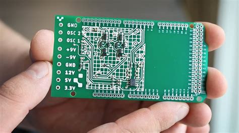
Heavy copper PCBs, characterized by their thick copper layers, have become increasingly significant in the USA electronics industry. These specialized printed circuit boards offer a range of advantages that make them indispensable in various applications, particularly those requiring high power and thermal management. As the demand for more robust and reliable electronic components grows, the role of heavy copper PCBs becomes even more crucial.
One of the primary advantages of heavy copper PCBs is their ability to handle high current loads.
Traditional PCBs, with their thinner copper layers, often struggle to manage the increased current demands of modern electronic devices. In contrast, heavy copper PCBs can efficiently conduct higher currents without overheating or suffering from performance degradation. This capability is particularly beneficial in power electronics, where efficient current distribution is essential for optimal performance and longevity.
Moreover, heavy copper PCBs excel in thermal management, a critical factor in the design and operation of electronic devices.
The thicker copper layers facilitate better heat dissipation, reducing the risk of overheating and potential damage to components. This enhanced thermal performance is especially valuable in applications such as power supplies, automotive electronics, and industrial equipment, where maintaining stable operating temperatures is vital for reliability and safety.
In addition to their electrical and thermal advantages, heavy copper PCBs offer improved mechanical strength.
The robust construction of these PCBs makes them more resistant to physical stress and environmental factors, such as vibration and temperature fluctuations. This durability ensures that devices incorporating heavy copper PCBs can withstand harsh operating conditions, making them ideal for use in demanding environments like aerospace and military applications.
Furthermore, the versatility of heavy copper PCBs allows for more complex and compact designs.
Engineers can integrate multiple functions into a single board, reducing the overall size and weight of electronic devices. This capability is increasingly important as the industry moves towards miniaturization and the development of more compact and portable devices. By enabling more efficient use of space, heavy copper PCBs contribute to the advancement of innovative technologies and products.
The economic benefits of heavy copper PCBs should not be overlooked.
While the initial cost of manufacturing these boards may be higher than that of standard PCBs, their long-term advantages often result in cost savings. The enhanced reliability and durability of heavy copper PCBs reduce the need for frequent repairs and replacements, leading to lower maintenance costs over the lifespan of the device. Additionally, their ability to handle higher power levels can result in energy savings, further contributing to their cost-effectiveness.
In conclusion, heavy copper PCBs offer a multitude of advantages that make them a valuable asset in the USA electronics industry. Their superior current handling capabilities, excellent thermal management, enhanced mechanical strength, and design versatility position them as a preferred choice for a wide range of applications. As the industry continues to evolve and demand for more efficient and reliable electronic components increases, the importance of heavy copper PCBs is likely to grow, driving further innovation and development in this critical area.
Manufacturing Process Of Heavy Copper PCBs In The USA
The manufacturing process of heavy copper PCBs in the USA is a sophisticated and intricate procedure that demands precision and expertise. Heavy copper PCBs, characterized by their thick copper layers, are essential in applications requiring high current or enhanced thermal management.
The process begins with the selection of high-quality raw materials, which is crucial for ensuring the reliability and performance of the final product.
Typically, the base material consists of a dielectric substrate, often made from FR-4, which is then laminated with copper foil. The thickness of the copper foil is significantly greater than that used in standard PCBs, often exceeding 3 ounces per square foot.
Once the materials are prepared, the next step involves the design and layout of the PCB.
Advanced computer-aided design (CAD) software is employed to create precise patterns that will be transferred onto the copper layers. This stage is critical, as it determines the electrical pathways and the overall functionality of the PCB. Following the design phase, the process moves to the etching stage, where unwanted copper is removed to reveal the desired circuit patterns. This is achieved through a chemical etching process, which must be carefully controlled to ensure accuracy and prevent over-etching, which could compromise the integrity of the circuit.
Subsequently, the PCBs undergo a plating process to enhance the thickness of the copper traces.
Electroplating is commonly used, where the boards are submerged in a solution containing copper ions. An electric current is then applied, causing the copper ions to deposit onto the existing traces, thereby increasing their thickness. This step is particularly important for heavy copper PCBs, as it ensures that the boards can handle higher currents and provide better thermal management.
Following plating, the boards are subjected to a series of drilling operations to create holes for component leads and vias.
Precision drilling machines are used to ensure that the holes are accurately positioned and of the correct diameter. After drilling, the boards undergo a cleaning process to remove any debris or contaminants that may have accumulated during the previous steps.
The next phase involves the application of a solder mask, which is a protective layer that prevents solder from bridging between conductive traces and causing short circuits.
The solder mask is typically applied using a screen-printing process, followed by curing under ultraviolet light. This step not only protects the copper traces but also enhances the overall durability of the PCB.
Finally, the boards are subjected to a series of rigorous testing procedures to ensure their functionality and reliability.
Electrical tests are conducted to verify the integrity of the circuits, while thermal tests assess the board’s ability to dissipate heat effectively. Only after passing these stringent tests are the heavy copper PCBs deemed ready for deployment in various industrial applications.
In conclusion, the manufacturing process of heavy copper PCBs in the USA is a complex and meticulous endeavor that requires advanced technology and skilled craftsmanship. From the selection of raw materials to the final testing phase, each step is carefully executed to produce PCBs that meet the demanding requirements of high-power and high-reliability applications. As technology continues to evolve, the demand for heavy copper PCBs is expected to grow, further underscoring the importance of this specialized manufacturing process.
Applications Of Heavy Copper PCBs In The USA Market
Heavy copper PCBs, characterized by their thick copper layers, have become increasingly significant in the USA market due to their unique properties and versatile applications. These printed circuit boards are distinguished by copper weights exceeding three ounces per square foot, which endows them with enhanced durability and superior thermal management capabilities. As industries continue to demand more robust and efficient electronic components, heavy copper PCBs have emerged as a critical solution, particularly in sectors where reliability and performance are paramount.
One of the primary applications of heavy copper PCBs in the USA is in the power electronics industry.
These PCBs are integral to the design and manufacture of power supplies, converters, and distribution systems. The ability of heavy copper PCBs to handle high current loads without overheating makes them ideal for these applications. They ensure efficient power distribution and minimize energy loss, which is crucial for maintaining the performance and longevity of power electronic devices. Moreover, their robust construction allows them to withstand the mechanical stresses and thermal cycling often encountered in power applications, thereby enhancing the reliability of the entire system.
In addition to power electronics, heavy copper PCBs are extensively used in the automotive industry.
As vehicles become more technologically advanced, the demand for reliable electronic components has surged. Heavy copper PCBs are employed in various automotive applications, including electric vehicle charging systems, power steering, and braking systems. Their ability to manage high currents and dissipate heat effectively ensures that these critical systems operate safely and efficiently. Furthermore, the automotive sector’s shift towards electric and hybrid vehicles has further amplified the need for heavy copper PCBs, as these vehicles require sophisticated power management systems to function optimally.
The renewable energy sector in the USA also benefits significantly from heavy copper PCBs.
With the growing emphasis on sustainable energy solutions, solar and wind power systems have become increasingly prevalent. Heavy copper PCBs are used in the inverters and converters that form the backbone of these renewable energy systems. Their capacity to handle high power levels and operate reliably under extreme environmental conditions makes them indispensable in this context. By facilitating efficient energy conversion and distribution, heavy copper PCBs contribute to the overall efficiency and reliability of renewable energy installations.
Moreover, heavy copper PCBs find applications in the aerospace and defense industries, where performance and reliability are non-negotiable.
These sectors demand electronic components that can endure harsh environments and operate flawlessly under high-stress conditions. Heavy copper PCBs meet these requirements by offering exceptional thermal management and mechanical strength. They are used in a variety of applications, including radar systems, communication devices, and avionics, where their ability to maintain performance under extreme conditions is critical.
In conclusion, the applications of heavy copper PCBs in the USA market are diverse and expanding. Their unique properties make them indispensable in industries that require high performance, reliability, and efficiency. As technological advancements continue to drive the demand for more sophisticated electronic components, the role of heavy copper PCBs is likely to grow even further. By providing solutions that meet the stringent requirements of various sectors, heavy copper PCBs are poised to remain a cornerstone of the electronics industry in the USA.

Innovations In Heavy Copper PCB Technology In The USA
In recent years, the landscape of printed circuit board (PCB) technology has witnessed significant advancements, particularly in the realm of heavy copper PCBs. These innovations have been pivotal in addressing the growing demands for more robust and reliable electronic components, especially in high-power applications. The United States, a leader in technological innovation, has been at the forefront of these developments, driving the evolution of heavy copper PCB technology to new heights.
Heavy copper PCBs, characterized by their thick copper layers, are designed to handle higher currents and provide enhanced thermal management.
This makes them ideal for applications in power electronics, automotive, and renewable energy sectors, where durability and performance are paramount. The increased copper thickness, often exceeding 3 ounces per square foot, allows these PCBs to withstand higher temperatures and mechanical stresses, thereby extending the lifespan of the electronic devices they support.
One of the key innovations in heavy copper PCB technology in the USA is the development of advanced fabrication techniques.
Traditional etching methods, which are often limited by their precision and efficiency, have been supplemented by more sophisticated processes such as laser etching and additive manufacturing. These techniques allow for greater accuracy in the production of complex circuit patterns, reducing material waste and improving overall production efficiency. Moreover, the integration of computer-aided design (CAD) software has streamlined the design process, enabling engineers to create intricate PCB layouts with ease and precision.
In addition to fabrication advancements, material science has played a crucial role in the evolution of heavy copper PCBs.
Researchers in the USA have been exploring new copper alloys and composite materials that offer superior electrical and thermal conductivity. These materials not only enhance the performance of heavy copper PCBs but also contribute to their sustainability by reducing the environmental impact of their production. Furthermore, the development of high-temperature laminates and substrates has expanded the operational range of these PCBs, making them suitable for use in extreme environments.
The demand for heavy copper PCBs has also spurred innovations in testing and quality assurance.
In the USA, manufacturers are employing state-of-the-art testing equipment to ensure that their products meet stringent industry standards. Advanced testing methods, such as X-ray inspection and automated optical inspection (AOI), have become integral to the production process, allowing for the detection of defects and ensuring the reliability of the final product. This focus on quality assurance is critical, as it instills confidence in consumers and reinforces the reputation of American-made heavy copper PCBs as being synonymous with excellence.
Moreover, the collaboration between industry and academia in the USA has been instrumental in driving research and development in heavy copper PCB technology.
Universities and research institutions are working closely with manufacturers to explore new applications and improve existing technologies. This synergy has led to the creation of innovative solutions that address the challenges faced by various industries, thereby expanding the potential uses of heavy copper PCBs.
In conclusion, the innovations in heavy copper PCB technology in the USA are a testament to the country’s commitment to advancing electronic manufacturing. Through cutting-edge fabrication techniques, material science breakthroughs, rigorous testing protocols, and collaborative research efforts, the USA continues to lead the way in developing heavy copper PCBs that meet the ever-evolving needs of modern technology. As these innovations continue to unfold, they promise to shape the future of electronics, paving the way for more efficient, reliable, and sustainable solutions.