Heavy copper pcb manufacturer
Advantages Of Heavy Copper PCB In The USA Electronics Industry
Heavy copper printed circuit boards (PCBs) have emerged as a pivotal component in the USA electronics industry, offering a multitude of advantages that cater to the evolving demands of modern technology. As the industry continues to push the boundaries of innovation, the need for robust and reliable components becomes increasingly critical. Heavy copper PCBs, characterized by their thick copper layers, provide a solution that addresses several challenges faced by electronic manufacturers today.
One of the primary advantages of heavy copper PCBs is their enhanced current-carrying capacity.
In applications where high power is a necessity, such as in power supplies, automotive electronics, and industrial controls, the ability to handle large currents without overheating is crucial. The thick copper layers in these PCBs allow for efficient heat dissipation, reducing the risk of thermal failure and ensuring the longevity of the electronic components. This capability is particularly beneficial in the USA, where industries are increasingly focused on developing energy-efficient and high-performance electronic systems.
Moreover, heavy copper PCBs offer superior mechanical strength, which is essential for applications subjected to harsh environmental conditions.
The robust construction of these PCBs makes them resistant to thermal cycling and mechanical stress, thereby enhancing their reliability and durability. This is especially important in sectors such as aerospace and defense, where equipment is often exposed to extreme temperatures and vibrations. By utilizing heavy copper PCBs, manufacturers can ensure that their products meet stringent reliability standards, a critical factor in maintaining competitiveness in the global market.
In addition to their mechanical and thermal advantages, heavy copper PCBs also contribute to improved electrical performance.
The thick copper layers reduce the risk of conductor loss, which can lead to signal degradation in high-frequency applications. This is particularly advantageous in the telecommunications industry, where maintaining signal integrity is paramount. As the USA continues to expand its telecommunications infrastructure, the demand for components that can support high-speed data transmission is on the rise. Heavy copper PCBs provide a reliable solution that meets these requirements, facilitating the development of advanced communication systems.
Furthermore, the versatility of heavy copper PCBs allows for innovative design possibilities.
Engineers can integrate multiple copper weights on a single board, enabling the creation of complex circuits that can accommodate both high-power and low-power components. This flexibility is invaluable in the design of compact and efficient electronic devices, which are increasingly sought after in the consumer electronics market. As the USA electronics industry continues to prioritize miniaturization and multifunctionality, heavy copper PCBs offer a means to achieve these goals without compromising on performance or reliability.
In conclusion, the advantages of heavy copper PCBs in the USA electronics industry are manifold. Their ability to handle high currents, withstand harsh conditions, and maintain electrical performance makes them an indispensable component in a wide range of applications. As technological advancements continue to drive the demand for more sophisticated electronic systems, the role of heavy copper PCBs is likely to become even more significant. By leveraging the benefits of these robust and versatile components, the USA electronics industry can continue to innovate and maintain its position at the forefront of global technological development.
Manufacturing Process Of Heavy Copper PCBs In The USA
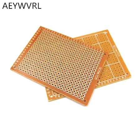
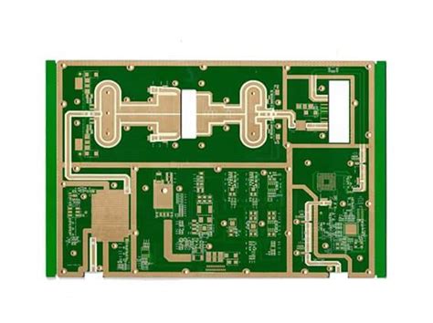
The manufacturing process of heavy copper PCBs in the USA is a sophisticated and intricate procedure that demands precision and expertise. Heavy copper PCBs, characterized by their thick copper layers, are essential in applications requiring high current or enhanced thermal management. The process begins with the selection of high-quality raw materials, which is crucial to ensure the reliability and performance of the final product. Copper-clad laminates are typically used as the base material, and the thickness of the copper layer can range from 3 oz/ft² to over 20 oz/ft², depending on the specific requirements of the application.
Once the materials are selected, the next step involves the design and layout of the PCB.
Advanced computer-aided design (CAD) software is employed to create precise and detailed designs that meet the stringent specifications required for heavy copper PCBs. This stage is critical, as any errors in the design can lead to significant issues in the final product. After the design is finalized, the manufacturing process moves to the etching stage, where unwanted copper is removed to create the desired circuit patterns. This is achieved through a series of chemical processes that carefully etch away the excess copper without damaging the underlying substrate.
Following the etching process, the PCBs undergo a series of drilling operations to create holes for component leads and vias.
These holes are then plated with copper to ensure electrical connectivity between different layers of the PCB. The plating process is particularly important in heavy copper PCBs, as it must accommodate the increased thickness of the copper layers. This is achieved through electroplating, where a layer of copper is deposited onto the drilled holes, ensuring robust and reliable connections.
Subsequently, the PCBs are subjected to a solder mask application, which involves coating the board with a protective layer to prevent solder bridges and protect against environmental factors.
The solder mask is typically applied using a screen-printing process, followed by curing to ensure durability. This step is essential in maintaining the integrity of the PCB during the soldering of components and throughout its operational life.
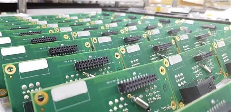
The final stages of the manufacturing process involve the application of surface finishes and the assembly of components.
Surface finishes, such as HASL (Hot Air Solder Leveling) or ENIG (Electroless Nickel Immersion Gold), are applied to protect the exposed copper and enhance solderability. The choice of finish depends on the specific application and performance requirements of the PCB. Once the surface finish is applied, components are mounted onto the PCB using automated pick-and-place machines, followed by soldering to secure them in place.
Quality control is a critical aspect of the manufacturing process, ensuring that each PCB meets the required standards and specifications.
Rigorous testing, including electrical testing and visual inspections, is conducted to identify any defects or inconsistencies. This ensures that the heavy copper PCBs produced in the USA are of the highest quality, capable of withstanding demanding applications and environments.
In conclusion, the manufacturing process of heavy copper PCBs in the USA is a complex and meticulous procedure that combines advanced technology with skilled craftsmanship. From the selection of materials to the final assembly and testing, each step is carefully executed to produce PCBs that meet the highest standards of performance and reliability. This process not only highlights the technical expertise required but also underscores the importance of quality control in delivering superior products to the market.
Applications Of Heavy Copper PCBs In American Technology Sectors
Heavy copper PCBs, characterized by their thick copper layers, have become increasingly significant in various American technology sectors due to their enhanced durability and superior thermal management capabilities. These printed circuit boards, which typically feature copper thicknesses ranging from 3 oz/ft² to over 20 oz/ft², are particularly valued for their ability to handle high current loads and dissipate heat efficiently. As a result, they are finding applications in a wide array of industries, each benefiting from the unique properties that heavy copper PCBs offer.
In the renewable energy sector, heavy copper PCBs are indispensable.
Solar power systems, for instance, require components that can withstand high current and voltage levels. Heavy copper PCBs are ideal for this purpose, as they can efficiently manage the thermal and electrical demands of solar inverters and converters. This capability not only enhances the reliability of solar power systems but also extends their lifespan, making them more cost-effective in the long run. Similarly, in wind energy applications, these PCBs are used in power converters and control systems, where their robustness ensures consistent performance under varying environmental conditions.
Transitioning to the automotive industry, the rise of electric vehicles (EVs) has further underscored the importance of heavy copper PCBs.
EVs demand high-performance electronic components that can handle substantial power loads while maintaining safety and efficiency. Heavy copper PCBs are employed in battery management systems, power steering, and braking systems, where their ability to manage high currents and dissipate heat is crucial. This not only improves the performance of electric vehicles but also contributes to their safety and reliability, which are paramount in automotive applications.
Moreover, the telecommunications sector in the United States also benefits significantly from heavy copper PCBs.
As the demand for faster and more reliable communication networks grows, so does the need for robust infrastructure. Heavy copper PCBs are used in power amplifiers and base stations, where they support high-frequency signals and manage the associated thermal loads. This ensures that communication networks remain stable and efficient, even under heavy usage, thereby supporting the ever-increasing data demands of modern society.
In addition to these sectors, heavy copper PCBs are also crucial in the aerospace and defense industries.
These sectors require components that can endure extreme conditions, including high temperatures and mechanical stress. Heavy copper PCBs are used in power supplies, radar systems, and other critical applications where reliability is non-negotiable. Their ability to withstand harsh environments while maintaining performance makes them an invaluable asset in these high-stakes industries.
Furthermore, the medical technology sector in the United States is increasingly adopting heavy copper PCBs.
Medical devices often require precise and reliable electronic components to ensure patient safety and effective treatment. Heavy copper PCBs are used in imaging systems, diagnostic equipment, and life-support devices, where their durability and thermal management capabilities are essential. This ensures that medical devices operate accurately and consistently, which is vital for patient care.
In conclusion, heavy copper PCBs play a pivotal role across various American technology sectors, offering unmatched durability and thermal management. Their applications in renewable energy, automotive, telecommunications, aerospace, defense, and medical technology underscore their versatility and importance. As technology continues to advance, the demand for heavy copper PCBs is likely to grow, further cementing their place as a cornerstone of modern electronic systems.
Innovations In Heavy Copper PCB Design By USA Companies
In recent years, the demand for heavy copper printed circuit boards (PCBs) has surged, driven by their ability to handle higher currents and provide enhanced thermal management. This demand has spurred significant innovations in heavy copper PCB design, particularly by companies based in the United States. These advancements are not only meeting the needs of industries such as automotive, aerospace, and renewable energy but are also setting new standards in PCB manufacturing.
One of the primary innovations in heavy copper PCB design is the development of advanced fabrication techniques.
Traditional PCB manufacturing processes often struggle to accommodate the increased thickness of copper layers, which can range from 3 ounces per square foot to over 20 ounces. However, U.S. companies have pioneered methods such as the use of specialized etching and plating techniques that allow for precise control over copper deposition. This precision ensures that the PCBs can handle high current loads without compromising structural integrity or performance.
Moreover, American companies have been at the forefront of integrating heavy copper PCBs with other advanced materials to enhance their functionality.
For instance, the incorporation of thermal management materials, such as metal cores or heat sinks, has become increasingly common. These materials work in tandem with the heavy copper layers to dissipate heat more effectively, thereby improving the reliability and lifespan of electronic components. This integration is particularly beneficial in applications where thermal performance is critical, such as in electric vehicles or high-power LED systems.
In addition to material innovations, design software advancements have played a crucial role in the evolution of heavy copper PCBs.
U.S. companies have invested heavily in developing sophisticated design tools that allow engineers to simulate and optimize PCB layouts before fabrication. These tools enable the precise modeling of electrical and thermal properties, ensuring that the final product meets stringent performance criteria. By leveraging these software solutions, designers can minimize potential issues such as electromagnetic interference or signal loss, which are particularly challenging in high-current applications.
Furthermore, the focus on sustainability and environmental responsibility has influenced the design and manufacturing processes of heavy copper PCBs in the United States.
Companies are increasingly adopting eco-friendly practices, such as using lead-free solder and implementing recycling programs for copper waste. These initiatives not only reduce the environmental impact of PCB production but also align with the growing demand for sustainable electronics solutions.
The collaboration between U.S. companies and academic institutions has also been instrumental in driving innovation in heavy copper PCB design.
Research partnerships have led to the exploration of novel materials and fabrication techniques, resulting in breakthroughs that have been rapidly adopted by the industry. This synergy between academia and industry ensures a continuous flow of new ideas and technologies, keeping U.S. companies at the cutting edge of PCB design.
In conclusion, the innovations in heavy copper PCB design by U.S. companies are a testament to the country’s leadership in the electronics manufacturing sector. Through advancements in fabrication techniques, material integration, design software, and sustainable practices, these companies are not only meeting the current demands of high-power applications but are also paving the way for future developments. As industries continue to evolve and require more robust and efficient electronic solutions, the role of heavy copper PCBs will undoubtedly become even more significant, with U.S. companies leading the charge in innovation and excellence.