Biggest circuit board in the world
Evolution Of The World’s Largest Circuit Board
The evolution of the world’s largest circuit board is a fascinating journey that reflects the rapid advancements in technology and the ever-growing demand for more powerful and efficient electronic devices. Circuit boards, also known as printed circuit boards (PCBs), are the backbone of modern electronics, providing the necessary pathways for electrical currents to flow between various components.
Over the years, the size and complexity of these boards have increased significantly, driven by the need to accommodate more components and enhance performance.
Initially, circuit boards were relatively simple, with limited functionality and a small number of components.
As technology progressed, the demand for more sophisticated devices led to the development of larger and more complex PCBs. This evolution was fueled by the miniaturization of electronic components, which allowed for more elements to be packed onto a single board. Consequently, the size of circuit boards began to grow, not only in terms of physical dimensions but also in terms of the number of layers and the complexity of the circuitry.
The quest for the largest circuit board is not merely about size; it is also about the ability to integrate a vast array of components and functionalities into a single platform.
This integration is crucial for applications in various fields, including telecommunications, computing, and industrial automation. As industries continue to push the boundaries of what is possible, the need for larger and more capable circuit boards becomes increasingly apparent.
One of the key factors driving the development of larger circuit boards is the rise of data centers and cloud computing.
These facilities require immense processing power and storage capacity, which in turn necessitates the use of large, multi-layered PCBs. These boards must be capable of handling high-speed data transfer and processing, while also being able to dissipate the significant amounts of heat generated by the components.
As a result, engineers and designers are constantly innovating to create circuit boards that can meet these demanding requirements.
Moreover, the automotive industry has also contributed to the evolution of large circuit boards. With the advent of electric and autonomous vehicles, the need for advanced electronic systems has grown exponentially.
These vehicles rely on complex PCBs to manage everything from battery management systems to advanced driver-assistance systems (ADAS). The integration of these systems into a single, cohesive platform requires circuit boards that are not only large but also highly reliable and efficient.
In addition to these industries, the aerospace and defense sectors have also played a significant role in the development of the world’s largest circuit boards.
The need for robust and reliable electronic systems in these fields is paramount, as they are often used in critical applications where failure is not an option. Consequently, the circuit boards used in these sectors are designed to withstand extreme conditions and provide unparalleled performance.
As we look to the future, the evolution of the world’s largest circuit board is likely to continue, driven by the relentless pursuit of technological advancement.
With the ongoing development of new materials and manufacturing techniques, the possibilities for even larger and more complex circuit boards are virtually limitless. This evolution will undoubtedly lead to new innovations and applications, further cementing the importance of circuit boards in our increasingly connected world.

Technological Innovations Behind The Biggest Circuit Board
The realm of technological innovation is constantly evolving, with each advancement pushing the boundaries of what is possible. Among these groundbreaking developments is the creation of the biggest circuit board in the world, a marvel of engineering that exemplifies the pinnacle of modern electronics.
This monumental achievement is not merely a testament to human ingenuity but also a reflection of the collaborative efforts that drive technological progress.
To understand the significance of this colossal circuit board, it is essential to delve into the intricacies of its design and construction.
Circuit boards, or printed circuit boards (PCBs), serve as the backbone of electronic devices, providing the necessary pathways for electrical currents to flow between components. The largest circuit board ever constructed is a feat of engineering that required meticulous planning and precision. It was designed to accommodate an unprecedented number of components, each meticulously arranged to optimize performance and efficiency.
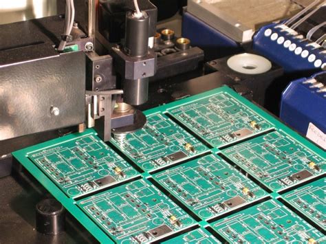
The creation of such a massive circuit board necessitated the use of cutting-edge materials and manufacturing techniques.
Advanced composite materials were employed to ensure the board’s structural integrity while maintaining its electrical conductivity. These materials were chosen for their ability to withstand the thermal and mechanical stresses that accompany the operation of such a large and complex system.
Furthermore, the manufacturing process involved state-of-the-art machinery capable of producing the intricate patterns required for the board’s functionality.
In addition to the materials and manufacturing techniques, the design of the circuit board itself posed significant challenges.
Engineers had to consider factors such as signal integrity, power distribution, and thermal management, all of which become increasingly complex as the size of the board increases. To address these challenges, sophisticated computer-aided design (CAD) software was utilized, allowing engineers to simulate and optimize the board’s performance before it was physically constructed. This software enabled the identification and resolution of potential issues, ensuring that the final product met the highest standards of quality and reliability.
The applications of the world’s largest circuit board are as impressive as its construction.
It is designed to support high-performance computing systems, which are essential for tasks such as data analysis, artificial intelligence, and scientific research.
The board’s expansive size allows it to house a vast array of processors and memory modules, providing the computational power necessary to tackle some of the most demanding challenges in these fields. Moreover, its design facilitates efficient cooling and power distribution, ensuring that the system operates at peak performance without overheating or experiencing power fluctuations.
The development of the biggest circuit board in the world is a testament to the collaborative efforts of engineers, scientists, and manufacturers.
It highlights the importance of interdisciplinary cooperation in achieving technological breakthroughs.
By combining expertise from various fields, these professionals were able to overcome the numerous challenges associated with designing and constructing such a complex system.
In conclusion, the creation of the largest circuit board in the world represents a significant milestone in the field of electronics. It showcases the potential of human innovation and the power of collaboration in pushing the boundaries of what is possible. As technology continues to advance, it is likely that we will see even more impressive feats of engineering, each building upon the achievements of those that came before. This circuit board not only serves as a functional component of high-performance computing systems but also as an inspiration for future generations of engineers and innovators.

Applications And Impact Of The Largest Circuit Board
The development of the largest circuit board in the world marks a significant milestone in the field of electronics, offering a plethora of applications and potential impacts across various industries. This monumental achievement is not merely a testament to human ingenuity and technological advancement but also a harbinger of transformative changes in how electronic systems are designed and utilized. As we delve into the applications and impacts of this colossal circuit board, it becomes evident that its influence extends far beyond its sheer size.
To begin with, the largest circuit board is poised to revolutionize the computing industry.
With its expansive surface area, it can accommodate an unprecedented number of components, thereby enhancing computational power and efficiency.
This capability is particularly beneficial for data centers, which require robust and efficient systems to manage vast amounts of information.
By integrating more processors and memory units onto a single board, data centers can achieve higher processing speeds and improved energy efficiency, ultimately leading to cost savings and reduced environmental impact.
Moreover, the implications for the telecommunications sector are equally profound.
The ability to house more components on a single board facilitates the development of more sophisticated communication systems. This advancement can lead to improved signal processing and transmission capabilities, which are crucial for the deployment of next-generation networks such as 5G and beyond. As a result, consumers can expect faster and more reliable connectivity, which is essential for the proliferation of the Internet of Things (IoT) and smart city initiatives.
In addition to computing and telecommunications, the largest circuit board holds promise for the aerospace and defense industries.
The integration of multiple systems onto a single board can lead to significant weight and space savings, which are critical factors in the design of aircraft and spacecraft. This innovation can enhance the performance and efficiency of these vehicles, enabling longer missions and more complex operations. Furthermore, the increased reliability and reduced complexity associated with a single-board system can improve the safety and robustness of critical defense applications.
Transitioning to the realm of consumer electronics, the impact of the largest circuit board is equally noteworthy.
As devices become increasingly compact and multifunctional, the demand for more efficient circuit designs grows. The ability to integrate more features onto a single board can lead to the development of more powerful and versatile gadgets, from smartphones to wearable technology. This trend not only enhances user experience but also drives innovation in product design and functionality.
While the applications of the largest circuit board are vast, it is important to consider the potential challenges and implications of its widespread adoption.
The complexity of designing and manufacturing such a large board requires advanced techniques and materials, which may pose technical and economic challenges. Additionally, the increased concentration of components on a single board raises concerns about heat dissipation and reliability, necessitating the development of new cooling solutions and testing methodologies.
In conclusion, the largest circuit board in the world represents a remarkable achievement with far-reaching applications and impacts across multiple industries. Its potential to enhance computational power, improve communication systems, and drive innovation in various fields underscores its significance in the ever-evolving landscape of technology. As researchers and engineers continue to explore its capabilities and address associated challenges, the largest circuit board is poised to play a pivotal role in shaping the future of electronics and beyond.
Challenges In Designing The World’s Biggest Circuit Board
Designing the world’s biggest circuit board presents a unique set of challenges that require innovative solutions and meticulous planning. As technology advances and the demand for more complex electronic systems grows, engineers are tasked with creating circuit boards that can accommodate an increasing number of components while maintaining functionality and reliability. The sheer size of the largest circuit board introduces several technical and logistical hurdles that must be addressed to ensure successful implementation.
One of the primary challenges in designing such a massive circuit board is managing the intricate network of electrical connections.
As the size of the board increases, so does the complexity of routing the numerous traces that connect various components. Ensuring that these connections are efficient and free from interference is crucial to maintaining the board’s performance.
Engineers must employ advanced computer-aided design (CAD) tools to simulate and optimize the layout, taking into account factors such as signal integrity, electromagnetic compatibility, and thermal management.
Moreover, the physical size of the circuit board poses significant manufacturing challenges.
Traditional fabrication processes may not be suitable for producing such large boards, necessitating the development of specialized techniques and equipment. For instance, the handling and transportation of oversized boards require careful consideration to prevent damage during production and assembly.
Additionally, ensuring uniformity in the application of solder paste and the placement of components across a vast surface area demands precision and consistency, which can be difficult to achieve on a large scale.
Another critical aspect to consider is the thermal management of the circuit board.
As electronic components generate heat during operation, effective heat dissipation becomes increasingly important to prevent overheating and ensure the longevity of the board. In the case of the world’s largest circuit board, engineers must design innovative cooling solutions that can efficiently manage the thermal load across the entire board. This may involve the integration of heat sinks, fans, or even liquid cooling systems, each of which must be carefully engineered to fit within the board’s design constraints.
Furthermore, the reliability and durability of the circuit board are paramount, especially when it is intended for use in critical applications such as aerospace, telecommunications, or data centers.
The board must be able to withstand environmental stresses, including temperature fluctuations, humidity, and mechanical vibrations. To achieve this, engineers must select materials that offer the necessary strength and resilience while also being compatible with the board’s electrical requirements.
Rigorous testing and quality assurance processes are essential to identify potential weaknesses and ensure that the board meets the highest standards of performance and safety.
In addition to these technical challenges, the economic implications of designing and producing the world’s largest circuit board cannot be overlooked. The cost of materials, manufacturing, and testing can be substantial, necessitating careful budget management and cost-effective design strategies. Collaboration between engineers, manufacturers, and suppliers is crucial to optimize resources and minimize expenses without compromising on quality.
In conclusion, the creation of the world’s biggest circuit board is a testament to human ingenuity and the relentless pursuit of technological advancement. By overcoming the myriad challenges associated with its design and production, engineers are paving the way for more sophisticated and powerful electronic systems that will shape the future of technology. Through innovation and collaboration, the boundaries of what is possible continue to be pushed, demonstrating the remarkable potential of modern engineering.