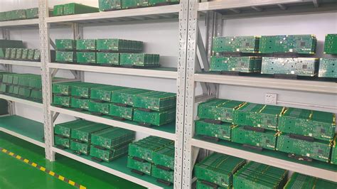
Files required for pcb manufacturing
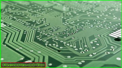
Gerber Files: The Blueprint of PCB Manufacturing
In the intricate world of printed circuit board (PCB) manufacturing, Gerber files stand as the quintessential blueprint, guiding the entire production process. These files, named after the Gerber Scientific Instrument Company, are the industry standard for conveying detailed information about the PCB design to manufacturers. Understanding the significance and composition of Gerber files is crucial for anyone involved in the design and production of PCBs, as they ensure precision and accuracy in translating a digital design into a physical product.
At the heart of PCB manufacturing, Gerber files serve as a comprehensive set of instructions that detail every aspect of the board’s design.
They are essentially a collection of files, each representing a different layer or component of the PCB. These files include information about the copper layers, solder mask, silkscreen, and drill data, among others. By providing a clear and detailed representation of each layer, Gerber files enable manufacturers to accurately reproduce the designer’s vision.
The copper layer files are perhaps the most critical, as they define the electrical pathways on the PCB.
These files specify the layout of the conductive traces, pads, and vias that form the circuit. Precision in these files is paramount, as any deviation can lead to electrical failures or suboptimal performance. Transitioning from the copper layers, the solder mask files are equally important. They define the areas on the PCB that should be covered with solder mask, a protective layer that prevents solder bridges and short circuits. The solder mask files ensure that only the necessary areas are exposed for soldering, thereby enhancing the board’s reliability.
In addition to the copper and solder mask layers, silkscreen files provide valuable information for assembly and troubleshooting.
These files contain text and symbols printed on the PCB surface, offering guidance on component placement and orientation. The silkscreen layer is essential for both the assembly process and future maintenance, as it helps technicians identify components and understand the board’s layout.
Moreover, drill files are a vital component of the Gerber file set.
They specify the locations and sizes of holes to be drilled into the PCB, which are necessary for mounting components and establishing electrical connections between layers. Accurate drill files are crucial to ensure that components fit correctly and that the board functions as intended.
To facilitate seamless communication between designers and manufacturers, Gerber files must adhere to specific standards.
The RS-274X format is the most widely used, offering a robust and flexible framework for representing PCB designs. This format supports a wide range of features, including apertures, layers, and attributes, making it suitable for complex designs.
In conclusion, Gerber files are the cornerstone of PCB manufacturing, providing a detailed and standardized blueprint for translating digital designs into physical boards. By encompassing all aspects of the PCB, from copper traces to drill holes, these files ensure that manufacturers can accurately and efficiently produce high-quality PCBs. As the industry continues to evolve, the importance of Gerber files remains steadfast, underscoring their role as an indispensable tool in the world of electronics manufacturing. Understanding and utilizing these files effectively is essential for anyone seeking to navigate the complexities of PCB production.
Drill Files: Ensuring Precision in PCB Fabrication
In the intricate world of printed circuit board (PCB) manufacturing, precision is paramount. Among the myriad of files required for successful PCB fabrication, drill files hold a place of critical importance. These files, often referred to as Excellon files, are essential for defining the locations, sizes, and types of holes that need to be drilled into the PCB. Understanding the role and requirements of drill files is crucial for ensuring the accuracy and functionality of the final product.
To begin with, drill files serve as a blueprint for the drilling process, which is a fundamental step in PCB manufacturing.
They provide detailed instructions to the drilling machines, specifying where each hole should be placed. This precision is vital because the holes are used for various purposes, such as mounting components, creating vias for electrical connections between layers, and accommodating mechanical fasteners. Any deviation from the specified locations can lead to misalignment, affecting the performance and reliability of the PCB.
Moreover, drill files contain information about the diameter of each hole.
This is particularly important because different components require different hole sizes. For instance, through-hole components, which have leads that pass through the board, necessitate larger holes compared to vias, which are used to connect different layers of the PCB. By accurately defining the hole sizes, drill files ensure that components fit correctly and maintain the integrity of electrical connections.
In addition to location and size, drill files also specify the type of hole to be drilled.
This includes distinguishing between plated and non-plated holes. Plated holes have a conductive coating that allows for electrical connectivity between layers, while non-plated holes do not. The distinction is crucial for the functionality of the PCB, as it determines how electrical signals are routed through the board. Therefore, drill files must clearly indicate the plating requirements for each hole to avoid any potential issues during the manufacturing process.
Transitioning to the technical aspects, drill files are typically generated using computer-aided design (CAD) software.
This software translates the design specifications into a format that can be interpreted by the drilling machines. The most common format for drill files is the Excellon format, which is widely accepted in the industry. This format includes a series of commands and coordinates that guide the drilling process, ensuring that each hole is drilled with precision.
Furthermore, it is essential to verify the accuracy of drill files before they are sent to the manufacturer.
This involves checking for any discrepancies or errors that could affect the drilling process. For instance, overlapping holes or incorrect coordinates can lead to defects in the PCB, resulting in costly rework or even complete failure of the board. By conducting a thorough review of the drill files, designers can identify and rectify any issues, thereby minimizing the risk of errors during fabrication.
In conclusion, drill files are a vital component of PCB manufacturing, providing the necessary instructions for precise hole placement, sizing, and type. Their accuracy directly impacts the functionality and reliability of the final product. By understanding the importance of drill files and ensuring their precision, manufacturers can produce high-quality PCBs that meet the stringent demands of modern electronic applications. As technology continues to advance, the role of drill files in achieving precision in PCB fabrication remains as crucial as ever.
Bill of Materials (BOM): The Essential Component List for PCBs
In the intricate world of printed circuit board (PCB) manufacturing, the Bill of Materials (BOM) stands as a crucial document that serves as the backbone for the entire production process. This essential component list is not merely a collection of parts; it is a comprehensive guide that ensures the seamless assembly and functionality of the PCB. Understanding the significance of the BOM is vital for anyone involved in the design and manufacturing of PCBs, as it directly impacts the efficiency, cost, and success of the final product.
To begin with, the BOM is a detailed inventory that enumerates all the components required to construct a PCB.
It includes information such as part numbers, descriptions, quantities, and specifications. This document acts as a bridge between the design and manufacturing phases, providing manufacturers with the necessary details to procure and assemble the components accurately. Without a well-structured BOM, the risk of errors and delays in the production process increases significantly, potentially leading to costly setbacks.
Moreover, the BOM plays a pivotal role in cost estimation and budgeting.
By listing all the components and their respective quantities, it allows manufacturers to calculate the total cost of materials needed for production. This financial foresight is crucial for project planning and management, enabling stakeholders to make informed decisions regarding resource allocation and pricing strategies. Additionally, a precise BOM can help identify opportunities for cost savings, such as bulk purchasing or substituting components with more cost-effective alternatives, without compromising on quality.
In addition to its financial implications, the BOM is instrumental in ensuring quality control and compliance with industry standards.
By providing detailed specifications for each component, it helps maintain consistency and reliability in the manufacturing process. This is particularly important in industries where adherence to strict standards is mandatory, such as aerospace, automotive, and medical devices. A meticulously prepared BOM can prevent the use of counterfeit or substandard components, thereby safeguarding the integrity and performance of the final product.
Furthermore, the BOM facilitates effective communication and collaboration among various stakeholders involved in the PCB manufacturing process.
Designers, engineers, procurement teams, and manufacturers rely on the BOM to share a common understanding of the project requirements. This shared knowledge base helps streamline workflows, reduce misunderstandings, and enhance overall productivity. In an increasingly globalized industry, where teams may be dispersed across different locations, the BOM serves as a universal reference point that aligns all parties towards a common goal.
As technology continues to evolve, the complexity of PCBs and their associated BOMs is also increasing.
Modern PCBs often incorporate a wide range of components, from traditional resistors and capacitors to advanced microprocessors and sensors. Consequently, the BOM must be meticulously organized and regularly updated to reflect any changes in design or component availability. Utilizing specialized software tools can aid in managing this complexity, ensuring that the BOM remains accurate and up-to-date throughout the product lifecycle.
In conclusion, the Bill of Materials is an indispensable document in PCB manufacturing, serving as a comprehensive guide that underpins the entire production process. Its role in cost estimation, quality control, and stakeholder communication cannot be overstated. As the industry continues to advance, the importance of a well-prepared BOM will only grow, making it an essential tool for ensuring the success and reliability of PCB projects.
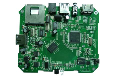
Assembly Drawings: Guiding the PCB Assembly Process
In the intricate world of printed circuit board (PCB) manufacturing, assembly drawings play a pivotal role in guiding the assembly process. These drawings serve as a comprehensive blueprint, ensuring that each component is accurately placed and soldered onto the board. As the complexity of electronic devices continues to grow, the importance of precise assembly drawings cannot be overstated. They provide a visual representation of the PCB, detailing the exact location and orientation of each component, which is crucial for both manual and automated assembly processes.
To begin with, assembly drawings typically include a top and bottom view of the PCB, offering a complete overview of the board’s layout.
These views are essential for understanding the spatial arrangement of components, which is critical for efficient assembly. Moreover, the drawings often incorporate a bill of materials (BOM), which lists all the components required for the assembly. This list is meticulously cross-referenced with the drawings to ensure that the correct components are used, thereby minimizing the risk of errors during assembly.
In addition to the visual layout, assembly drawings also provide detailed information about the components themselves.
This includes specifications such as part numbers, reference designators, and polarity indicators. Such details are vital for ensuring that components are correctly oriented and connected, as even a minor misalignment can lead to significant functional issues. Furthermore, these drawings often highlight critical areas of the PCB, such as test points and connectors, which require special attention during assembly.
Transitioning to the next aspect, it is important to note that assembly drawings are not static documents.
They are dynamic tools that evolve alongside the design and manufacturing processes. As design changes occur, the drawings must be updated to reflect these modifications. This iterative process ensures that the assembly team always has access to the most current and accurate information, thereby facilitating a smooth and efficient assembly process.
Moreover, assembly drawings serve as a vital communication tool between the design and manufacturing teams.
They bridge the gap between the conceptual design and the physical assembly, translating complex design specifications into actionable instructions. This communication is crucial for maintaining consistency and quality throughout the manufacturing process. By providing a clear and detailed roadmap, assembly drawings help to align the efforts of various teams, ensuring that everyone is working towards the same goal.
In addition to guiding the assembly process, these drawings also play a significant role in quality control.
They serve as a reference point for inspecting the assembled PCB, allowing quality control teams to verify that each component is correctly placed and soldered. This verification process is essential for identifying and rectifying any assembly errors before the PCB moves on to the next stage of production.
In conclusion, assembly drawings are an indispensable component of the PCB manufacturing process.
They provide a detailed and accurate representation of the PCB, guiding the assembly process and ensuring that each component is correctly placed and oriented. By facilitating communication between design and manufacturing teams, these drawings help to maintain consistency and quality throughout the production process. As electronic devices continue to evolve, the role of assembly drawings in ensuring precise and efficient PCB assembly will only become more critical.