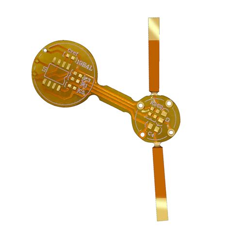
Flex foil pcb
Advantages Of Using Flex Foil PCB In Modern Electronics
Flex foil printed circuit boards (PCBs) have emerged as a pivotal innovation in the realm of modern electronics, offering a multitude of advantages that cater to the evolving demands of contemporary technology. As electronic devices become increasingly compact and complex, the need for flexible, reliable, and efficient circuit solutions has never been more critical. Flex foil PCBs, with their unique properties, address these needs by providing a versatile platform that enhances both the design and functionality of electronic devices.
One of the primary advantages of flex foil PCBs is their inherent flexibility, which allows them to be bent, folded, or twisted without compromising their performance.
This flexibility is particularly beneficial in applications where space is at a premium, such as in wearable technology, medical devices, and compact consumer electronics. By enabling circuits to conform to non-traditional shapes and spaces, flex foil PCBs facilitate innovative design possibilities that rigid PCBs simply cannot accommodate. Consequently, designers can create more ergonomic and aesthetically pleasing products that meet the demands of modern consumers.
In addition to their flexibility, flex foil PCBs offer significant weight and space savings.
Traditional rigid PCBs often require additional connectors and cables to achieve the same level of functionality, which can add bulk and weight to the final product. Flex foil PCBs, on the other hand, integrate these components into a single, streamlined design, reducing the overall footprint and weight of the device. This is particularly advantageous in applications such as aerospace and automotive industries, where every gram counts and space is limited.
Moreover, flex foil PCBs are known for their durability and reliability.
The materials used in their construction, such as polyimide or polyester films, are resistant to extreme temperatures, moisture, and chemicals, making them suitable for use in harsh environments. This resilience ensures that devices equipped with flex foil PCBs maintain their performance over time, even under challenging conditions. Furthermore, the reduced need for connectors and solder joints in flex foil PCBs minimizes potential points of failure, enhancing the overall reliability of the electronic device.
Another noteworthy advantage of flex foil PCBs is their ability to improve signal integrity.
The continuous nature of the conductive paths in flex foil PCBs reduces the risk of signal loss or interference, which is a common issue in traditional rigid PCBs with multiple interconnections. This characteristic is particularly important in high-frequency applications, where maintaining signal quality is crucial for optimal performance. As a result, flex foil PCBs are increasingly being utilized in telecommunications and data transmission equipment, where signal integrity is paramount.
In conclusion, the advantages of using flex foil PCBs in modern electronics are manifold, encompassing flexibility, weight and space efficiency, durability, and improved signal integrity. As technology continues to advance and the demand for more compact, reliable, and efficient electronic devices grows, the role of flex foil PCBs is set to become even more significant. By enabling innovative designs and enhancing device performance, flex foil PCBs are not only meeting the current needs of the electronics industry but are also paving the way for future technological advancements.
Design Considerations For Flex Foil PCB Applications
When designing flex foil PCBs, several critical considerations must be taken into account to ensure optimal performance and reliability. Flex foil PCBs, known for their ability to bend and conform to various shapes, are increasingly used in applications where space constraints and mechanical flexibility are paramount. As such, understanding the unique design requirements of these circuits is essential for engineers and designers.
To begin with, material selection plays a pivotal role in the design of flex foil PCBs.
The choice of substrate material affects not only the flexibility but also the thermal and electrical properties of the circuit. Polyimide is a popular choice due to its excellent thermal stability and flexibility. However, depending on the specific application, other materials such as polyester may be considered for their cost-effectiveness and adequate performance in less demanding environments. The thickness of the substrate also influences the flexibility and durability of the PCB, necessitating a careful balance between mechanical strength and pliability.
In addition to material considerations, the layout design of flex foil PCBs requires meticulous attention.
The routing of traces should be optimized to minimize stress and potential failure points. Curved traces are preferred over sharp angles, as they distribute mechanical stress more evenly across the board. Furthermore, the use of staggered vias and teardrop pads can enhance the mechanical integrity of the connections, reducing the risk of cracking or delamination under repeated flexing.
Thermal management is another crucial aspect of flex foil PCB design.
Due to their compact nature, these circuits can be prone to overheating, which can degrade performance and lead to failure. Incorporating thermal vias and heat-dissipating materials can help manage heat distribution effectively. Additionally, designers should consider the placement of components to ensure that heat-sensitive parts are adequately shielded from high-temperature areas.
Moreover, the choice of adhesive and coverlay materials is vital in protecting the circuitry from environmental factors such as moisture, dust, and mechanical abrasion.
The coverlay not only serves as a protective layer but also contributes to the overall flexibility of the PCB. Selecting an adhesive that maintains its properties under varying temperatures and mechanical stress is essential for long-term reliability.
Transitioning to the electrical performance, impedance control is a significant consideration in flex foil PCB design, especially for high-frequency applications.
The flexible nature of these circuits can introduce variations in impedance, which can affect signal integrity. To mitigate this, designers must carefully calculate trace widths and spacing, taking into account the dielectric properties of the substrate. Implementing controlled impedance techniques ensures that the circuit meets the required electrical specifications.
Finally, manufacturability and cost are important factors that influence design decisions.
While flex foil PCBs offer numerous advantages, they can be more expensive to produce than traditional rigid PCBs. Therefore, designers must weigh the benefits of flexibility against the potential increase in manufacturing costs. Collaborating with manufacturers early in the design process can help identify cost-effective solutions and streamline production.
In conclusion, designing flex foil PCBs involves a comprehensive understanding of material properties, mechanical and thermal considerations, and electrical performance requirements. By addressing these factors thoughtfully, engineers can create flexible circuits that meet the demands of modern electronic applications, ensuring both functionality and durability.

Manufacturing Process Of Flex Foil PCB: A Step-By-Step Guide
The manufacturing process of flex foil printed circuit boards (PCBs) is a sophisticated and intricate procedure that requires precision and expertise. Flex foil PCBs, known for their flexibility and lightweight properties, are increasingly used in various applications, from consumer electronics to aerospace technology. Understanding the step-by-step process of their production is essential for appreciating the complexity and innovation involved in their creation.
To begin with, the process starts with the selection of the base material, which is typically a flexible substrate such as polyimide.
This material is chosen for its excellent thermal stability and flexibility, which are crucial for the performance of the final product. Once the substrate is selected, it is thoroughly cleaned to remove any impurities that could affect the adhesion of the subsequent layers.
Following the preparation of the substrate, the next step involves the application of a conductive layer, usually copper, onto the substrate.
This is achieved through a process called lamination, where the copper foil is bonded to the substrate under heat and pressure. The thickness of the copper layer is carefully controlled to ensure optimal electrical performance while maintaining flexibility.
Subsequently, the laminated material undergoes a process known as photolithography.
In this step, a photosensitive resist is applied to the copper surface, and a photomask is used to expose specific areas to ultraviolet light. The exposed areas are then developed, revealing the desired circuit pattern. This pattern is crucial as it dictates the electrical pathways on the PCB.
Once the circuit pattern is established, the next phase is etching.
During etching, the unwanted copper is removed, leaving behind only the copper traces that form the circuit. This is typically done using a chemical solution that dissolves the unprotected copper. The precision of this step is vital, as any errors can lead to circuit failures.
After etching, the remaining photoresist is stripped away, and the board is cleaned to remove any residues.
At this point, the flex foil PCB begins to take shape, but additional processes are necessary to enhance its functionality and durability. One such process is the application of a solder mask, which is a protective layer that insulates the copper traces and prevents short circuits. The solder mask is applied using a similar photolithographic process to ensure accuracy.
Following the application of the solder mask, the next step is the addition of surface finishes.
These finishes, such as gold or silver, are applied to the exposed copper pads to protect them from oxidation and to ensure reliable soldering during component assembly. The choice of finish depends on the specific requirements of the application.
Finally, the flex foil PCB undergoes a series of inspections and tests to ensure it meets the required specifications and quality standards. These tests include electrical testing to verify circuit continuity and functionality, as well as visual inspections to check for any physical defects.
In conclusion, the manufacturing process of flex foil PCBs is a meticulous and multi-step procedure that combines advanced materials and precise engineering techniques. Each step, from substrate preparation to final testing, is crucial in producing a high-quality product that meets the demands of modern technology. As the demand for flexible and lightweight electronic solutions continues to grow, the importance of understanding and mastering this process becomes ever more significant.
Flex Foil PCB Vs. Rigid PCB: Key Differences And Applications
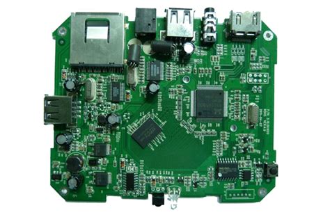
Flex foil PCBs and rigid PCBs are two distinct types of printed circuit boards that serve different purposes in the electronics industry. Understanding the key differences between these two types of PCBs is crucial for selecting the appropriate one for specific applications. Flex foil PCBs, also known as flexible PCBs, are designed to be bent and shaped to fit into compact and irregular spaces. This flexibility is achieved through the use of flexible substrates, such as polyimide, which allow the circuit to conform to the desired shape without compromising its functionality. In contrast, rigid PCBs are made from solid materials like fiberglass, which provide a stable and inflexible platform for electronic components.
One of the primary differences between flex foil PCBs and rigid PCBs lies in their construction and material composition.
Flex foil PCBs are constructed using thin layers of conductive copper and insulating materials that can withstand bending and twisting. This unique construction allows them to be used in applications where space is limited or where the circuit needs to move or flex during operation. On the other hand, rigid PCBs are built with multiple layers of copper and fiberglass, providing a sturdy and durable structure that is ideal for applications requiring a stable and permanent circuit board.
The applications of flex foil PCBs and rigid PCBs further highlight their differences.
Flex foil PCBs are commonly used in devices where space and weight are critical factors, such as in smartphones, wearable technology, and medical devices. Their ability to bend and conform to tight spaces makes them ideal for these applications, where traditional rigid PCBs would be impractical. Additionally, flex foil PCBs are often used in automotive and aerospace industries, where they can withstand vibrations and dynamic movements without failure.
In contrast, rigid PCBs are typically used in applications where stability and durability are paramount.
They are commonly found in desktop computers, televisions, and other consumer electronics that require a solid and reliable circuit board. The rigidity of these PCBs ensures that the components remain securely in place, reducing the risk of damage or malfunction. Furthermore, rigid PCBs are often used in industrial and military applications, where they can withstand harsh environments and provide consistent performance over time.
Despite their differences, both flex foil PCBs and rigid PCBs offer unique advantages that make them suitable for specific applications.
Flex foil PCBs provide the flexibility and adaptability needed for compact and dynamic devices, while rigid PCBs offer the stability and durability required for more robust applications. When choosing between these two types of PCBs, it is essential to consider the specific requirements of the application, including factors such as space constraints, environmental conditions, and the need for flexibility or rigidity.
In conclusion, the choice between flex foil PCBs and rigid PCBs depends largely on the intended application and the specific needs of the project. By understanding the key differences in their construction, material composition, and applications, designers and engineers can make informed decisions that optimize the performance and reliability of their electronic devices. As technology continues to evolve, the demand for both types of PCBs will likely grow, driven by the increasing complexity and diversity of electronic applications.