Flex pcb diy
Introduction To Flex PCB DIY: Understanding The Basics
Flexible printed circuit boards, commonly known as flex PCBs, have become an integral component in modern electronics due to their versatility and adaptability. As technology continues to advance, the demand for compact and efficient electronic solutions has led to the increased popularity of flex PCBs. For enthusiasts and professionals alike, understanding the basics of flex PCB DIY is essential for harnessing their full potential. This article aims to provide a comprehensive introduction to the world of flex PCB DIY, offering insights into their structure, benefits, and the initial steps required to embark on a DIY project.
To begin with, it is important to understand what distinguishes flex PCBs from their rigid counterparts.
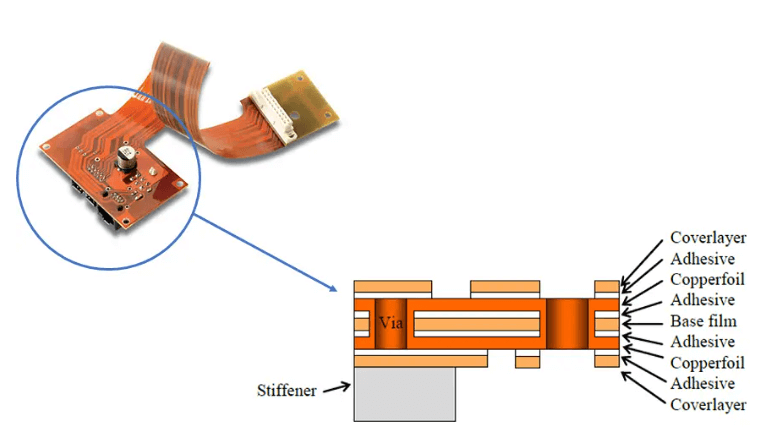
Unlike traditional rigid PCBs, which are made from inflexible materials such as fiberglass, flex PCBs are constructed using flexible plastic substrates like polyimide. This flexibility allows them to be bent, folded, and twisted without damaging the circuitry, making them ideal for applications where space is limited or where the board needs to conform to a specific shape. Consequently, flex PCBs are widely used in a variety of industries, including consumer electronics, automotive, and medical devices.
The benefits of using flex PCBs extend beyond their physical flexibility.
They offer significant advantages in terms of weight reduction and space savings, as they can replace multiple rigid boards and connectors with a single, streamlined design. This not only reduces the overall weight of the device but also minimizes the risk of connection failures, thereby enhancing reliability. Furthermore, flex PCBs can improve signal integrity by reducing the number of interconnections and providing a more direct path for electrical signals.
For those interested in exploring flex PCB DIY, it is crucial to start with a clear understanding of the design and fabrication process.
The first step involves designing the circuit layout using specialized software tools. These tools allow users to create intricate designs that take full advantage of the flexibility offered by flex PCBs. It is essential to consider factors such as bend radius, component placement, and trace routing to ensure the final product meets the desired specifications.
Once the design is finalized, the next phase involves selecting the appropriate materials.
The choice of substrate, adhesive, and conductive materials will depend on the specific requirements of the project, such as temperature resistance, electrical conductivity, and mechanical durability. It is advisable to consult with material suppliers or manufacturers to ensure the selected materials are compatible with the intended application.
Following material selection, the fabrication process begins.
This typically involves several steps, including etching, drilling, and lamination, to create the desired circuit pattern on the flexible substrate. Due to the complexity of this process, many DIY enthusiasts opt to work with professional fabrication services that specialize in flex PCBs. These services can provide valuable expertise and ensure the final product meets industry standards.
In conclusion, flex PCB DIY offers a fascinating opportunity for individuals to engage with cutting-edge technology and create innovative electronic solutions. By understanding the fundamental principles of flex PCBs, including their structure, benefits, and design considerations, enthusiasts can embark on projects that push the boundaries of traditional electronics. As the demand for flexible and efficient electronic solutions continues to grow, mastering the basics of flex PCB DIY will undoubtedly prove to be a valuable skill in the ever-evolving landscape of technology.
Essential Tools And Materials For Flex PCB DIY Projects
Embarking on a flex PCB DIY project can be an exciting venture for electronics enthusiasts and professionals alike. Flex PCBs, or flexible printed circuit boards, offer a unique advantage over traditional rigid PCBs due to their ability to bend and conform to various shapes. This flexibility makes them ideal for applications where space is limited or where the circuit needs to fit into unconventional spaces. However, to successfully create and work with flex PCBs, it is crucial to have the right tools and materials at your disposal. Understanding the essential components required for such projects can significantly enhance the efficiency and quality of your work.
To begin with, a high-quality design software is indispensable.
Software such as Eagle, Altium Designer, or KiCad allows you to design the circuit layout with precision. These programs offer features that help in simulating the circuit’s performance, ensuring that the design is both functional and efficient before moving on to the physical creation. Transitioning from design to production, a reliable computer with sufficient processing power is necessary to handle these software applications smoothly.
Once the design is finalized, the next step involves transferring it onto the flex PCB material.
For this, a laser printer or a plotter is essential for printing the design onto a transfer film. This film is then used to imprint the design onto the copper-clad flex PCB material. The choice of flex PCB material is critical; polyimide is commonly used due to its excellent thermal stability and flexibility. It is important to select a material that matches the specific requirements of your project, considering factors such as temperature resistance and mechanical durability.
Etching the circuit is another crucial step in the process.
A good etching solution, typically ferric chloride or ammonium persulfate, is required to remove the unwanted copper from the board, leaving only the desired circuit pattern. Safety precautions are paramount when handling these chemicals, as they can be hazardous. Therefore, protective gear such as gloves and goggles should be worn at all times.
Drilling precise holes for component placement is another task that requires specialized tools.
A precision drill press or a Dremel tool with appropriate drill bits is necessary to create clean and accurate holes. This step is vital for ensuring that components fit correctly and maintain a secure connection with the board.
Soldering is an integral part of assembling the flex PCB.
A high-quality soldering iron with adjustable temperature settings is essential for working with the delicate materials involved. Additionally, using lead-free solder can be beneficial for both health and environmental reasons. A steady hand and a keen eye are required to ensure that components are soldered correctly without damaging the flexible substrate.
Finally, testing and troubleshooting tools such as a multimeter and an oscilloscope are indispensable for verifying the functionality of the completed flex PCB.
These tools help in identifying any issues in the circuit, allowing for timely corrections and ensuring that the final product meets the desired specifications.
In conclusion, undertaking a flex PCB DIY project requires a comprehensive set of tools and materials, each playing a crucial role in the successful creation of a functional and reliable circuit. By equipping yourself with the right resources and knowledge, you can navigate the complexities of flex PCB design and production with confidence and precision.
Step-By-Step Guide To Designing Your Own Flex PCB
Designing your own flexible printed circuit board (flex PCB) can be a rewarding endeavor, offering both the satisfaction of creating a custom solution and the potential for significant cost savings. To embark on this journey, it is essential to understand the fundamental steps involved in the design process. This guide aims to provide a comprehensive overview, ensuring that even those new to the field can approach the task with confidence.
To begin with, it is crucial to have a clear understanding of the requirements and constraints of your project.
This involves defining the electrical and mechanical specifications, such as the number of layers, the type of materials to be used, and the overall dimensions of the flex PCB. Additionally, consider the environmental conditions the board will be exposed to, as these factors will influence material selection and design choices. Once these parameters are established, you can proceed to the next phase of the design process.
The next step involves selecting the appropriate design software.
There are numerous options available, ranging from free, open-source programs to more advanced, professional-grade tools. The choice of software will depend on your specific needs and level of expertise. It is advisable to choose a program that offers robust support for flex PCB design, including features such as bend radius calculations and material stack-up management. With the software in hand, you can begin creating the schematic diagram, which serves as the blueprint for your circuit.
Transitioning from the schematic to the layout phase, it is important to pay attention to the unique challenges posed by flex PCBs.
Unlike rigid boards, flex PCBs must accommodate bending and flexing, which necessitates careful consideration of trace routing and component placement. To mitigate stress on the traces, it is advisable to use curved traces instead of sharp angles and to distribute components evenly across the board. Furthermore, incorporating teardrop pads at trace-to-pad junctions can enhance mechanical strength and reliability.
As you progress, it is essential to perform a thorough design rule check (DRC) to ensure that your layout adheres to the manufacturing constraints and industry standards.
This step helps identify potential issues such as trace width violations, spacing errors, and other design flaws that could compromise the functionality of the final product. Addressing these issues early in the design process can save time and resources in the long run.
Once the layout is finalized, the next step is to generate the necessary files for manufacturing.
This typically involves exporting Gerber files, which contain the information required for each layer of the PCB, as well as a bill of materials (BOM) and an assembly drawing. It is advisable to review these files carefully to ensure accuracy and completeness before submitting them to a manufacturer.
Finally, selecting a reputable manufacturer with experience in producing flex PCBs is crucial to the success of your project.
Communicate your requirements clearly and provide any additional documentation that may assist in the manufacturing process. Once the boards are produced, conduct a thorough inspection and testing to verify that they meet the desired specifications and perform as intended.
In conclusion, designing your own flex PCB involves a series of methodical steps, each requiring careful consideration and attention to detail. By following this guide and leveraging the right tools and resources, you can successfully create a custom flex PCB that meets your specific needs and applications.

Common Challenges And Solutions In Flex PCB DIY
Flex PCBs, or flexible printed circuit boards, have become increasingly popular in various applications due to their ability to bend and conform to different shapes. This adaptability makes them ideal for use in compact and complex electronic devices. However, when it comes to DIY projects, working with flex PCBs presents unique challenges that hobbyists and engineers alike must navigate. Understanding these challenges and their potential solutions is crucial for anyone looking to successfully incorporate flex PCBs into their projects.
One of the primary challenges in flex PCB DIY is the material handling.
Unlike rigid PCBs, flex PCBs are made from flexible materials such as polyimide, which can be more difficult to manage. These materials are prone to tearing and creasing, which can lead to circuit failure. To mitigate this issue, it is essential to handle the flex PCB with care, using tools specifically designed for flexible materials. Additionally, storing the flex PCBs in a flat, dry environment can prevent unwanted bending and moisture absorption, which can further compromise the material’s integrity.
Another significant challenge is the design complexity associated with flex PCBs.
The flexibility of these boards allows for intricate designs, but this also means that the design process can be more complicated. Designers must consider factors such as bend radius, dynamic flexing, and the potential for mechanical stress. To address these complexities, utilizing advanced design software that supports flex PCB design is recommended. This software can help in visualizing the board’s behavior under different conditions, allowing for more accurate and reliable designs.
Soldering components onto a flex PCB is another area where DIY enthusiasts may encounter difficulties.
The heat from soldering can damage the flexible substrate, leading to delamination or warping. To prevent this, it is advisable to use low-temperature soldering techniques and to apply heat for the shortest time possible. Additionally, using a soldering iron with a fine tip can help in achieving precision without applying excessive heat to the surrounding areas.
Moreover, ensuring reliable electrical connections on a flex PCB can be challenging due to the board’s movement and flexibility.
Over time, repeated bending can cause solder joints to crack or components to become loose. To enhance the durability of these connections, it is beneficial to use flexible adhesives or encapsulants that can absorb mechanical stress. These materials can provide additional support to the solder joints and components, reducing the risk of failure.
Testing and troubleshooting flex PCBs also pose unique challenges.
The flexible nature of these boards can make it difficult to secure them in a test fixture, leading to inaccurate readings. To overcome this, using specialized test fixtures designed for flex PCBs can ensure stable and reliable testing conditions. Additionally, employing non-contact testing methods, such as optical inspection, can help in identifying defects without physically stressing the board.
In conclusion, while flex PCB DIY projects present several challenges, understanding these issues and implementing appropriate solutions can lead to successful outcomes. By carefully handling materials, utilizing advanced design tools, employing precise soldering techniques, ensuring robust electrical connections, and adopting effective testing methods, hobbyists and engineers can fully leverage the benefits of flex PCBs in their innovative projects. As technology continues to advance, the demand for flexible electronics will likely grow, making the mastery of flex PCB DIY an increasingly valuable skill.