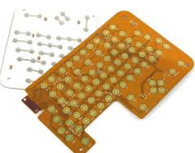
Flex pcb emi shielding
Understanding The Basics Of Flex PCB EMI Shielding
Electromagnetic interference (EMI) is a critical concern in the design and functionality of electronic devices, particularly as technology continues to advance and devices become more compact and complex. Flex PCBs, or flexible printed circuit boards, are increasingly utilized in modern electronics due to their adaptability and space-saving benefits. However, their flexible nature can make them more susceptible to EMI, necessitating effective shielding solutions to ensure optimal performance and reliability.
Understanding the basics of flex PCB EMI shielding involves recognizing the sources and impacts of electromagnetic interference.
EMI can originate from various sources, including other electronic components, power lines, and even natural phenomena such as lightning. This interference can disrupt the normal operation of electronic circuits, leading to data loss, signal degradation, and even complete device failure. Therefore, implementing effective EMI shielding is crucial to maintaining the integrity and functionality of electronic devices that incorporate flex PCBs.
The process of EMI shielding in flex PCBs typically involves the use of conductive materials that can block or absorb electromagnetic waves.
These materials are often applied as a coating or layer over the flex PCB, creating a barrier that prevents EMI from penetrating the circuit. Common materials used for this purpose include copper, aluminum, and conductive polymers, each offering different levels of effectiveness and suitability depending on the specific application and environmental conditions.
In addition to material selection, the design and layout of the flex PCB play a significant role in EMI shielding.
Careful consideration must be given to the placement of components and traces to minimize potential interference. For instance, maintaining adequate spacing between traces and components can reduce the likelihood of crosstalk, a form of EMI that occurs when signals from one trace interfere with those in another. Furthermore, incorporating ground planes and vias can enhance the shielding effectiveness by providing additional paths for electromagnetic waves to dissipate.
Another important aspect of flex PCB EMI shielding is the integration of shielding enclosures or covers.
These enclosures are typically made from metal or conductive materials and are designed to encase the entire circuit or specific components that are particularly sensitive to EMI. By enclosing these areas, the shielding enclosures provide an additional layer of protection against external electromagnetic fields, further safeguarding the device’s performance.
Moreover, the choice of adhesive and bonding techniques used in assembling flex PCBs can influence the effectiveness of EMI shielding.
Conductive adhesives, for example, can enhance the electrical connection between the shielding material and the PCB, ensuring a more robust barrier against interference. Additionally, the use of advanced bonding techniques can help maintain the flexibility of the PCB while still providing adequate protection against EMI.
In conclusion, understanding the basics of flex PCB EMI shielding is essential for engineers and designers working with modern electronic devices. By carefully selecting materials, optimizing design layouts, and incorporating effective shielding solutions, it is possible to mitigate the effects of electromagnetic interference and ensure the reliable operation of devices that rely on flex PCBs. As technology continues to evolve, the importance of effective EMI shielding will only grow, making it a critical consideration in the development of future electronic innovations.
Innovative Materials For Enhanced Flex PCB EMI Shielding
In the rapidly evolving landscape of electronics, the demand for flexible printed circuit boards (FPCBs) has surged, driven by their adaptability and lightweight nature. These attributes make FPCBs indispensable in a variety of applications, from consumer electronics to medical devices.
However, as electronic devices become more compact and complex, the challenge of electromagnetic interference (EMI) becomes increasingly pronounced.
EMI can disrupt the performance of electronic circuits, leading to malfunctions or degraded performance. Consequently, effective EMI shielding is crucial to ensure the reliability and functionality of FPCBs.
Traditionally, EMI shielding has been achieved through the use of metal enclosures or coatings. While effective, these methods often add weight and reduce the flexibility of the circuit board, counteracting the inherent advantages of FPCBs. Therefore, the development of innovative materials that provide robust EMI shielding while maintaining the flexibility and lightweight nature of FPCBs is of paramount importance. Recent advancements in material science have introduced a range of novel materials that address these challenges.
One promising approach involves the use of conductive polymers.
These materials offer the dual benefits of flexibility and conductivity, making them ideal candidates for EMI shielding in FPCBs. Conductive polymers can be applied as thin coatings, providing an effective barrier against electromagnetic interference without significantly increasing the weight or altering the flexibility of the circuit board. Moreover, these polymers can be engineered to exhibit specific electrical properties, allowing for tailored EMI shielding solutions that meet the unique requirements of different applications.
In addition to conductive polymers, nanomaterials have emerged as a groundbreaking solution for EMI shielding in FPCBs.
Materials such as graphene and carbon nanotubes possess exceptional electrical conductivity and mechanical strength, making them highly effective at blocking electromagnetic waves. When integrated into FPCBs, these nanomaterials form a conductive network that dissipates electromagnetic energy, thereby mitigating interference. Furthermore, the incorporation of nanomaterials can enhance the thermal management of FPCBs, addressing another critical aspect of electronic device performance.
Another innovative material gaining traction in the realm of EMI shielding is metalized fabrics.
These fabrics are composed of fibers coated with metals such as copper or nickel, providing excellent conductivity and shielding effectiveness. Metalized fabrics can be laminated onto FPCBs, offering a lightweight and flexible solution that does not compromise the board’s mechanical properties. Additionally, these fabrics can be designed to provide selective shielding, targeting specific frequency ranges to optimize performance.
The integration of these advanced materials into FPCBs not only enhances EMI shielding but also opens new avenues for design and functionality.
For instance, the use of flexible, lightweight materials allows for the development of wearable electronics and other applications where traditional rigid circuit boards would be impractical. As the demand for such applications continues to grow, the importance of innovative EMI shielding solutions will only increase.
In conclusion, the quest for effective EMI shielding in flexible printed circuit boards has led to significant advancements in material science. Conductive polymers, nanomaterials, and metalized fabrics represent just a few of the innovative materials that are transforming the landscape of FPCB design. By leveraging these materials, manufacturers can create electronic devices that are not only more reliable and efficient but also more versatile and adaptable to the needs of modern technology. As research and development in this field continue to progress, the potential for further innovation remains vast, promising exciting developments in the years to come.
Design Techniques To Optimize Flex PCB EMI Shielding
In the realm of modern electronics, the demand for compact and efficient devices has led to the increased use of flexible printed circuit boards (PCBs). These flexible PCBs offer numerous advantages, including reduced weight, space savings, and enhanced durability. However, as with any electronic component, they are susceptible to electromagnetic interference (EMI), which can degrade performance and reliability. Therefore, optimizing EMI shielding in flex PCBs is crucial to ensure their effective operation in various applications.
To begin with, understanding the sources of EMI is essential for designing effective shielding solutions.
EMI can originate from both external sources, such as nearby electronic devices, and internal sources, such as the components and traces on the PCB itself. Consequently, a comprehensive approach to EMI shielding must address both these aspects. One fundamental design technique involves the strategic placement of ground planes. Ground planes act as a barrier to EMI, providing a low-impedance path for noise to dissipate. By incorporating continuous ground planes in the flex PCB design, designers can significantly reduce the susceptibility to EMI.
Moreover, the use of shielding materials is another effective strategy.
Conductive materials, such as copper or aluminum, can be laminated onto the flex PCB to create a physical barrier against EMI. These materials can be applied as a solid layer or in a grid pattern, depending on the specific requirements of the application. Additionally, the thickness and conductivity of the shielding material play a crucial role in its effectiveness. Therefore, selecting the appropriate material and configuration is vital to achieving optimal EMI shielding.
In addition to material selection, the layout of the flex PCB is a critical factor in minimizing EMI.
Careful routing of traces can help reduce the potential for interference. For instance, keeping high-speed signal traces short and away from sensitive components can mitigate the risk of EMI. Furthermore, maintaining adequate spacing between traces and components can prevent crosstalk, which is a common source of EMI in densely packed circuits. By adhering to these layout principles, designers can enhance the overall EMI performance of the flex PCB.
Transitioning to another important aspect, the use of vias in flex PCBs can also influence EMI shielding.
Vias are used to connect different layers of the PCB, and their placement can impact the effectiveness of the ground plane. Ensuring that vias are properly placed and connected to the ground plane can help maintain a continuous shield against EMI. Additionally, using stitching vias, which are closely spaced vias connecting the ground planes, can further enhance the shielding effectiveness by reducing the loop area for EMI to penetrate.
Furthermore, the integration of EMI filters can be a valuable addition to the design.
These filters can be incorporated at critical points in the circuit to suppress unwanted noise. By selecting the appropriate filter type and configuration, designers can target specific frequency ranges and effectively mitigate EMI.
In conclusion, optimizing EMI shielding in flex PCBs requires a multifaceted approach that encompasses material selection, layout design, via placement, and the integration of filters. By employing these design techniques, engineers can enhance the performance and reliability of flex PCBs in various applications. As electronic devices continue to evolve, the importance of effective EMI shielding in flex PCBs will only grow, underscoring the need for innovative design solutions in this dynamic field.
Challenges And Solutions In Flex PCB EMI Shielding
In the realm of modern electronics, the demand for compact, lightweight, and flexible devices has led to the increased use of flexible printed circuit boards (flex PCBs). These innovative circuits offer numerous advantages, including the ability to bend and fold, which is particularly beneficial in applications where space is limited. However, as with any technological advancement, flex PCBs present their own set of challenges, one of the most significant being electromagnetic interference (EMI) shielding. EMI can disrupt the performance of electronic devices, leading to malfunctions or degraded performance. Therefore, effective EMI shielding is crucial to ensure the reliability and functionality of devices utilizing flex PCBs.
One of the primary challenges in flex PCB EMI shielding is the inherent flexibility of the material.
Traditional EMI shielding methods, such as metal enclosures or rigid coatings, are not suitable for flex PCBs due to their lack of flexibility. Consequently, engineers must explore alternative materials and techniques that can provide adequate shielding while maintaining the board’s flexibility. Conductive films and foils, for instance, have emerged as viable solutions. These materials can be laminated onto the flex PCB, offering a flexible yet effective barrier against electromagnetic interference. However, the application of these materials must be carefully controlled to avoid adding excessive weight or thickness, which could compromise the board’s flexibility.
Moreover, the integration of EMI shielding into flex PCBs must consider the thermal management of the device.
As electronic components become more densely packed, heat dissipation becomes a critical concern. Shielding materials can potentially impede heat flow, leading to overheating and reduced performance. To address this, engineers are exploring the use of thermally conductive yet electrically insulating materials that can provide both EMI shielding and efficient heat dissipation. This dual-functionality approach not only enhances the performance of the device but also extends its lifespan by preventing thermal damage.
In addition to material selection, the design of the flex PCB itself plays a crucial role in EMI shielding.
Strategic placement of ground planes and careful routing of signal traces can significantly reduce EMI susceptibility. By minimizing loop areas and ensuring proper grounding, engineers can mitigate the effects of electromagnetic interference. Furthermore, incorporating vias and stitching techniques can enhance the effectiveness of the shielding by providing multiple paths for grounding and reducing the potential for EMI leakage.
Despite these advancements, the implementation of EMI shielding in flex PCBs is not without its challenges.
The manufacturing process must be meticulously controlled to ensure the integrity of the shielding materials and the overall performance of the board. Variations in material properties, such as conductivity and thickness, can impact the effectiveness of the shielding, necessitating rigorous quality control measures. Additionally, the cost of advanced materials and manufacturing techniques can be a barrier for some applications, particularly in cost-sensitive markets.
In conclusion, while flex PCBs offer significant advantages in terms of design flexibility and space efficiency, they also present unique challenges in EMI shielding. Through the careful selection of materials, innovative design strategies, and precise manufacturing processes, engineers can overcome these challenges and ensure the reliable performance of devices utilizing flex PCBs. As technology continues to evolve, ongoing research and development will undoubtedly lead to even more effective solutions, further enhancing the capabilities of flex PCBs in a wide range of applications.