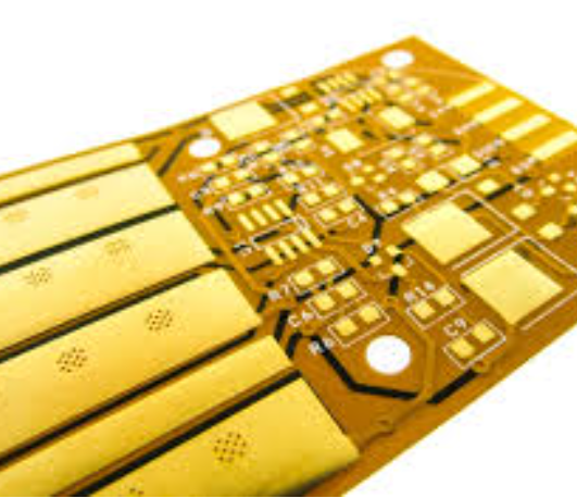
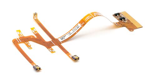
Flex pcb harness
Advantages Of Using Flex PCB Harness In Modern Electronics
In the rapidly evolving landscape of modern electronics, the demand for more compact, efficient, and reliable components has never been greater. One innovation that has significantly contributed to meeting these demands is the flex PCB harness. This technology offers a multitude of advantages that make it an indispensable component in contemporary electronic design and manufacturing.
To begin with, the inherent flexibility of flex PCB harnesses allows for a level of design versatility that rigid PCBs simply cannot match.
This flexibility enables the harness to be bent, folded, or twisted to fit into tight or irregular spaces, making it ideal for applications where space is at a premium. Consequently, this adaptability is particularly beneficial in the development of compact devices such as smartphones, wearable technology, and medical implants, where every millimeter counts.
Moreover, the use of flex PCB harnesses can lead to significant reductions in weight and size.
Traditional wiring systems often require multiple connectors and cables, which can add bulk and complexity to a device. In contrast, a flex PCB harness can integrate multiple functions into a single, streamlined component. This not only reduces the overall weight and size of the device but also simplifies the assembly process, leading to lower manufacturing costs and increased production efficiency. Additionally, the reduction in connectors and cables minimizes potential points of failure, thereby enhancing the reliability and longevity of the device.
Another notable advantage of flex PCB harnesses is their ability to withstand harsh environmental conditions.
The materials used in their construction are typically resistant to extreme temperatures, moisture, and chemicals, making them suitable for use in a wide range of challenging environments. This durability is particularly advantageous in industries such as automotive, aerospace, and industrial automation, where electronic components are often exposed to demanding conditions. Furthermore, the robust nature of flex PCB harnesses contributes to improved signal integrity. The continuous, uninterrupted pathways provided by these harnesses reduce the risk of signal loss or interference, which is crucial for maintaining the performance and accuracy of electronic systems.
In addition to these practical benefits, flex PCB harnesses also offer significant advantages in terms of design aesthetics.
The ability to create intricate, three-dimensional shapes allows designers to develop more innovative and visually appealing products. This is especially important in consumer electronics, where the look and feel of a device can be as important as its functionality. By enabling more creative design possibilities, flex PCB harnesses help manufacturers differentiate their products in a competitive market.
Finally, the use of flex PCB harnesses aligns with the growing emphasis on sustainability in the electronics industry.
The reduction in materials and energy required for their production, combined with their long lifespan, contributes to a lower environmental impact. As companies increasingly prioritize eco-friendly practices, the adoption of flex PCB harnesses represents a step towards more sustainable manufacturing processes.
In conclusion, the advantages of using flex PCB harnesses in modern electronics are manifold. From their unparalleled flexibility and space-saving properties to their durability and aesthetic potential, these components are revolutionizing the way electronic devices are designed and manufactured. As technology continues to advance, the role of flex PCB harnesses in shaping the future of electronics is set to become even more significant.
Design Considerations For Flex PCB Harness Applications
In the realm of modern electronics, the flex PCB harness has emerged as a pivotal component, offering a unique blend of flexibility and reliability. As technology continues to evolve, the demand for compact and efficient electronic solutions has led to the increased adoption of flexible printed circuit boards (PCBs). These components are particularly advantageous in applications where space constraints and dynamic movement are critical considerations. However, designing a flex PCB harness requires careful attention to several key factors to ensure optimal performance and longevity.
To begin with, understanding the mechanical properties of the materials used in flex PCBs is essential.
The choice of substrate material, typically polyimide, plays a crucial role in determining the flexibility and durability of the harness. Polyimide is favored for its excellent thermal stability and mechanical strength, which are vital in applications subjected to varying environmental conditions. Additionally, the copper traces on the flex PCB must be designed to withstand repeated bending and flexing. This involves selecting the appropriate copper thickness and ensuring that the traces are routed in a manner that minimizes stress concentration, thereby reducing the risk of fatigue failure.
Moreover, the layout of the flex PCB harness is another critical design consideration.
The routing of traces should be optimized to avoid sharp bends and corners, which can lead to stress points and potential failure. Instead, gradual curves and arcs are recommended to distribute mechanical stress more evenly across the board. Furthermore, the use of staggered vias and teardrop pads can enhance the mechanical integrity of the connections, providing additional support against mechanical stress.
In addition to mechanical considerations, electrical performance is a paramount concern in the design of flex PCB harnesses.
Signal integrity must be maintained to ensure reliable data transmission, especially in high-speed applications. This necessitates careful impedance control and the use of differential pair routing where applicable. Designers must also consider the potential for electromagnetic interference (EMI) and implement appropriate shielding techniques to mitigate its effects. This can include the use of ground planes and strategically placed decoupling capacitors to minimize noise and ensure stable operation.
Thermal management is another aspect that cannot be overlooked in the design of flex PCB harnesses.
The compact nature of these components often results in high power densities, which can lead to overheating if not properly managed. Effective thermal management strategies, such as the use of thermal vias and heat spreaders, are essential to dissipate heat and maintain the reliability of the harness. Additionally, selecting materials with high thermal conductivity can further enhance heat dissipation and prevent thermal-related failures.
Finally, manufacturability and cost considerations must be taken into account during the design process.
The complexity of the flex PCB harness design can significantly impact production costs and lead times. Therefore, designers should strive for a balance between performance requirements and manufacturability. This may involve simplifying the design where possible, without compromising on essential features, to facilitate efficient production and reduce costs.
In conclusion, the design of flex PCB harnesses is a multifaceted process that requires careful consideration of mechanical, electrical, thermal, and manufacturability factors. By addressing these considerations, designers can create robust and reliable flex PCB harnesses that meet the demands of modern electronic applications. As technology continues to advance, the importance of well-designed flex PCB harnesses will only grow, underscoring the need for continued innovation and attention to detail in their development.
Manufacturing Process Of Flex PCB Harness: A Step-By-Step Guide
The manufacturing process of a flex PCB harness is a meticulous and intricate procedure that requires precision and expertise. This process begins with the design phase, where engineers utilize advanced software to create detailed schematics and layouts. These designs are crucial as they dictate the electrical pathways and mechanical structure of the flex PCB harness. Once the design is finalized, it is transferred onto a flexible substrate, typically made of polyimide, which offers both flexibility and durability. This substrate serves as the foundation upon which the entire circuit is built.
Following the design transfer, the next step involves the application of a conductive material, usually copper, onto the substrate.
This is achieved through a process known as copper cladding, where a thin layer of copper is laminated onto the substrate. Subsequently, the unwanted copper is removed through a process called etching, leaving behind the desired circuit pattern. This step is critical as it forms the electrical pathways that will connect various components of the flex PCB harness.
After etching, the focus shifts to drilling, where precise holes are created in the substrate to accommodate vias and through-hole components.
These holes are essential for establishing electrical connections between different layers of the circuit. The drilling process is followed by plating, where the holes are coated with a conductive material to ensure reliable electrical connectivity. This step is vital for the overall functionality of the flex PCB harness, as it ensures seamless communication between different circuit layers.
Once the plating is complete, the flex PCB undergoes a solder mask application.
This involves coating the circuit with a protective layer that prevents solder bridges and short circuits during component assembly. The solder mask also enhances the durability of the flex PCB by protecting it from environmental factors such as moisture and dust. Following the solder mask application, a silkscreen layer is added to the flex PCB. This layer contains printed information such as component labels and reference indicators, which aid in the assembly and troubleshooting processes.
The next phase in the manufacturing process is component assembly, where various electronic components are mounted onto the flex PCB.
This is typically done using surface mount technology (SMT), which allows for the efficient placement of components onto the circuit. The components are then soldered in place, ensuring a secure and reliable connection. This step requires precision and accuracy, as any misalignment or poor soldering can compromise the performance of the flex PCB harness.
After assembly, the flex PCB harness undergoes rigorous testing to ensure its functionality and reliability.
This involves a series of electrical tests that verify the integrity of the circuit and the performance of the components. Any defects or issues identified during testing are addressed through rework or repair, ensuring that the final product meets the required quality standards.
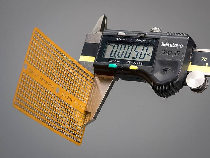
Finally, the flex PCB harness is subjected to a thorough inspection to ensure it meets all design specifications and quality requirements. This inspection includes visual checks and dimensional measurements to verify the accuracy of the manufacturing process. Once the flex PCB harness passes inspection, it is ready for integration into electronic devices, where its flexibility and reliability offer significant advantages in various applications. Through this comprehensive manufacturing process, flex PCB harnesses are produced with precision and quality, ensuring their effectiveness in modern electronic systems.
Common Challenges And Solutions In Flex PCB Harness Integration
In the realm of modern electronics, the integration of flexible printed circuit board (PCB) harnesses has become increasingly prevalent due to their ability to accommodate complex designs and compact spaces. However, this integration is not without its challenges. Understanding these challenges and their corresponding solutions is crucial for engineers and designers aiming to optimize the performance and reliability of their electronic devices.
One of the primary challenges in flex PCB harness integration is managing the mechanical stress that these components endure.
Flexible PCBs are often subjected to bending, twisting, and other forms of mechanical manipulation, which can lead to material fatigue and eventual failure. To address this, designers must carefully consider the bend radius and the number of flex cycles the PCB will undergo during its lifespan. Utilizing materials with high flexural endurance and incorporating strain relief features can significantly mitigate the risk of mechanical failure. Additionally, conducting thorough testing under simulated conditions can help identify potential weak points in the design.
Another significant challenge is ensuring signal integrity within the flex PCB harness.
As electronic devices become more sophisticated, the demand for high-speed data transmission increases, making signal integrity a critical concern. The flexible nature of these PCBs can introduce issues such as impedance mismatches and electromagnetic interference (EMI). To combat these problems, designers can employ techniques such as controlled impedance routing and the use of ground planes to minimize EMI. Furthermore, selecting appropriate materials with low dielectric constants can enhance signal performance, ensuring that data is transmitted accurately and efficiently.
Thermal management also poses a considerable challenge in the integration of flex PCB harnesses.
The compact nature of these components often results in limited space for heat dissipation, which can lead to overheating and reduced performance. To address this, engineers can incorporate thermal vias and heat sinks into the design to facilitate heat dissipation. Additionally, using materials with high thermal conductivity can help manage heat more effectively. Implementing active cooling solutions, such as fans or liquid cooling systems, may also be necessary in high-power applications to maintain optimal operating temperatures.
Moreover, the manufacturing process of flex PCB harnesses presents its own set of challenges.
The delicate nature of flexible materials requires precise handling and assembly techniques to prevent damage during production. Automated assembly processes, such as pick-and-place machines, can enhance precision and reduce the risk of human error. Additionally, employing advanced inspection methods, such as automated optical inspection (AOI) and X-ray inspection, can ensure that defects are identified and rectified early in the production process.
Finally, cost considerations cannot be overlooked in the integration of flex PCB harnesses.
The specialized materials and manufacturing processes required for these components can lead to higher production costs compared to traditional rigid PCBs. To mitigate these costs, designers can optimize the layout to minimize material usage and explore alternative materials that offer a balance between performance and cost. Collaborating with experienced manufacturers can also provide insights into cost-effective production techniques without compromising quality.
In conclusion, while the integration of flex PCB harnesses presents several challenges, understanding and addressing these issues is essential for successful implementation. By focusing on mechanical stress management, signal integrity, thermal management, manufacturing precision, and cost optimization, engineers can harness the full potential of flexible PCBs, paving the way for innovative and reliable electronic devices.