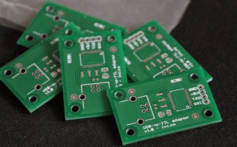
Flex pcb routing
Optimizing Signal Integrity in Flex PCB Routing
In the realm of modern electronics, the demand for compact, lightweight, and flexible devices has led to the increased adoption of flexible printed circuit boards (PCBs). These innovative circuits offer a myriad of advantages, including the ability to conform to complex shapes and withstand dynamic flexing. However, with these benefits come unique challenges, particularly in optimizing signal integrity during the routing process. Ensuring signal integrity in flex PCB routing is crucial, as it directly impacts the performance and reliability of electronic devices.
To begin with, understanding the fundamental differences between rigid and flexible PCBs is essential.
Unlike their rigid counterparts, flex PCBs are made from flexible substrates such as polyimide, which allows them to bend and twist. This flexibility, while advantageous, introduces potential issues such as signal distortion and electromagnetic interference (EMI). Therefore, careful consideration must be given to the routing process to mitigate these effects.
One of the primary factors affecting signal integrity in flex PCBs is the impedance of the traces.
Impedance mismatches can lead to signal reflections, which degrade the quality of the transmitted signal. To address this, designers must meticulously calculate and control the trace width, spacing, and thickness, as well as the dielectric constant of the substrate. By maintaining consistent impedance throughout the circuit, signal reflections can be minimized, thereby enhancing signal integrity.
Moreover, the layout of the traces plays a pivotal role in optimizing signal integrity.
It is advisable to keep trace lengths as short as possible to reduce the potential for signal loss and delay. Additionally, avoiding sharp bends and corners in the routing path can prevent impedance discontinuities, which are detrimental to signal quality. Instead, using smooth, gradual curves can help maintain a uniform impedance profile.
Transitioning to another critical aspect, the management of electromagnetic interference is paramount in flex PCB design.
EMI can be exacerbated by the proximity of traces to one another, leading to crosstalk and signal degradation. To mitigate this, designers should implement adequate spacing between traces and consider the use of ground planes or shielding layers. These measures can effectively reduce EMI and improve overall signal integrity.
Furthermore, the choice of materials in flex PCB construction significantly influences signal integrity.
High-quality substrates with low dielectric loss and stable dielectric constants are preferable, as they contribute to reduced signal attenuation and distortion. Additionally, selecting appropriate copper weights and finishes can enhance the electrical performance of the circuit.
In addition to these technical considerations, collaboration between design and manufacturing teams is essential to ensure optimal signal integrity.
Early involvement of manufacturers in the design process can provide valuable insights into material selection, fabrication techniques, and potential design constraints. This collaborative approach can lead to more robust and reliable flex PCB designs.
In conclusion, optimizing signal integrity in flex PCB routing requires a comprehensive understanding of the unique challenges posed by flexible circuits. By carefully managing impedance, trace layout, EMI, and material selection, designers can significantly enhance the performance and reliability of their electronic devices. As the demand for flexible electronics continues to grow, mastering these techniques will be crucial for engineers and designers striving to push the boundaries of innovation in the field.
Design Guidelines for Flex PCB Routing in Compact Devices
In the realm of modern electronics, the demand for compact and efficient devices has led to the increased utilization of flexible printed circuit boards (PCBs). These innovative components offer a unique advantage in terms of design flexibility, allowing for the creation of intricate circuits that can be bent and folded to fit into tight spaces. However, designing flex PCBs for compact devices requires careful consideration of several critical factors to ensure optimal performance and reliability.
To begin with, understanding the material properties of flex PCBs is essential.
Unlike rigid PCBs, flex PCBs are made from flexible substrates such as polyimide, which provide the necessary pliability. This flexibility, while advantageous, also introduces challenges in terms of mechanical stress and potential damage during bending. Therefore, it is crucial to select materials that can withstand repeated flexing without compromising the integrity of the circuit. Additionally, the thickness of the flex PCB should be minimized to enhance its flexibility, but not to the extent that it becomes too fragile.
Transitioning to the layout design, one must consider the routing of traces on the flex PCB.
The routing process should prioritize minimizing stress on the traces, especially in areas where the board will be bent or folded. To achieve this, designers should employ curved traces instead of sharp angles, as sharp angles can concentrate stress and lead to trace cracking. Furthermore, maintaining a consistent trace width and spacing is vital to prevent impedance mismatches and signal integrity issues, which are particularly critical in high-frequency applications.
Another important aspect of flex PCB routing is the placement of components.
In compact devices, space is at a premium, necessitating strategic component placement to optimize both functionality and manufacturability. Components should be positioned in such a way that they do not interfere with the bending areas of the flex PCB. Moreover, heavier components should be placed closer to the rigid sections of the board to reduce mechanical stress on the flexible areas. This strategic placement not only enhances the durability of the flex PCB but also facilitates easier assembly and testing.
In addition to component placement, the use of stiffeners is a common practice in flex PCB design.
Stiffeners are rigid materials added to specific areas of the flex PCB to provide additional support and prevent excessive bending. They are particularly useful in areas where connectors or other mechanical interfaces are located, as these regions are prone to higher mechanical stress. By incorporating stiffeners, designers can ensure that the flex PCB maintains its structural integrity while still allowing for the necessary flexibility in other areas.
Finally, it is imperative to consider the environmental conditions to which the flex PCB will be exposed.
Factors such as temperature fluctuations, humidity, and exposure to chemicals can all impact the performance and longevity of the flex PCB. Therefore, selecting materials and finishes that can withstand these conditions is crucial. Additionally, implementing protective coatings or encapsulation can provide an extra layer of defense against environmental stressors.
In conclusion, designing flex PCBs for compact devices involves a delicate balance between flexibility and durability. By carefully considering material selection, trace routing, component placement, and environmental factors, designers can create robust and reliable flex PCBs that meet the demands of modern compact electronic devices. Through meticulous planning and adherence to design guidelines, the potential of flex PCBs can be fully realized, paving the way for innovative and efficient electronic solutions.
Overcoming Common Challenges in Flex PCB Routing
Flex PCB routing presents a unique set of challenges that require careful consideration and strategic planning to overcome. As the demand for smaller, more efficient electronic devices continues to grow, the use of flexible printed circuit boards (PCBs) has become increasingly prevalent. These boards offer significant advantages, such as reduced weight and the ability to conform to complex shapes, making them ideal for a wide range of applications. However, the very characteristics that make flex PCBs desirable also introduce complexities in their design and manufacturing processes.
One of the primary challenges in flex PCB routing is managing the mechanical stress that these boards are subjected to during operation.
Unlike rigid PCBs, flex circuits must endure bending, twisting, and other forms of mechanical deformation. This necessitates a design approach that minimizes stress concentration points, which can lead to circuit failure. To address this, designers often employ techniques such as staggered vias and curved traces, which help distribute stress more evenly across the board. Additionally, selecting the appropriate materials that can withstand repeated flexing without degrading is crucial for ensuring the longevity and reliability of the circuit.
Another significant challenge is maintaining signal integrity in flex PCBs.
The flexible nature of these boards can lead to variations in impedance, which can adversely affect high-speed signal transmission. To mitigate this issue, designers must carefully control the trace width, spacing, and layer stack-up to ensure consistent impedance throughout the circuit. Moreover, incorporating ground planes and using differential signaling can help reduce electromagnetic interference and crosstalk, further enhancing signal integrity.
Thermal management is also a critical consideration in flex PCB routing.
The compact size and high component density of modern electronic devices can lead to significant heat generation, which must be effectively dissipated to prevent damage to the circuit. Flex PCBs often have limited options for heat dissipation due to their thin and flexible nature. Therefore, designers must employ innovative solutions such as thermal vias, heat sinks, and the use of thermally conductive materials to manage heat effectively. Additionally, simulating thermal performance during the design phase can help identify potential hotspots and allow for proactive design adjustments.
Furthermore, the manufacturing process of flex PCBs introduces its own set of challenges.
The thin and flexible substrates used in these boards can be difficult to handle and require specialized equipment and processes. Ensuring precise alignment and registration during fabrication is essential to avoid defects and ensure the functionality of the final product. Collaboration with experienced manufacturers who understand the nuances of flex PCB production can be invaluable in overcoming these challenges.
In conclusion, while flex PCB routing presents several challenges, they are not insurmountable.
By understanding the unique properties of flexible circuits and employing strategic design and manufacturing techniques, these challenges can be effectively addressed. As technology continues to advance, the demand for flex PCBs is likely to increase, making it essential for designers and manufacturers to stay abreast of the latest developments and best practices in this field. Through continuous innovation and collaboration, the potential of flex PCBs can be fully realized, enabling the creation of more advanced and efficient electronic devices.
Innovations in Flex PCB Routing for Wearable Technology
In recent years, the rapid advancement of wearable technology has necessitated significant innovations in the design and manufacturing of flexible printed circuit boards (PCBs). These innovations are crucial as they enable the seamless integration of electronic components into wearable devices, which demand both flexibility and durability. Flex PCBs, known for their ability to bend and conform to various shapes, are particularly well-suited for this purpose. As wearable technology continues to evolve, the routing of flex PCBs has become a focal point for engineers and designers seeking to optimize performance and reliability.
One of the primary challenges in flex PCB routing for wearable technology is the need to maintain signal integrity while accommodating the dynamic movements of the human body.
Traditional rigid PCBs are not suitable for wearables due to their inability to withstand bending and twisting. Flex PCBs, however, offer a solution by allowing circuits to be routed in a manner that can endure repeated mechanical stress. To achieve this, engineers have developed advanced routing techniques that minimize the risk of signal degradation. For instance, the use of serpentine traces, which are designed to absorb mechanical stress, has become a common practice. These traces allow the circuit to stretch and compress without compromising electrical performance.
Moreover, the miniaturization of electronic components has further influenced flex PCB routing strategies.
As wearable devices become smaller and more compact, the need for efficient use of space on the PCB becomes paramount. This has led to the adoption of high-density interconnect (HDI) technology, which allows for more components to be placed on a smaller area of the board. HDI technology utilizes microvias, blind vias, and buried vias to create multi-layered circuits that maximize space efficiency. Consequently, this innovation not only enhances the functionality of wearable devices but also contributes to their aesthetic appeal by enabling sleeker designs.
In addition to space optimization, thermal management is another critical consideration in flex PCB routing for wearables.
Wearable devices often operate in close proximity to the skin, making it essential to manage heat dissipation effectively. Engineers have addressed this challenge by incorporating thermal vias and heat-spreading materials into the PCB design. These features help to distribute heat evenly across the board, preventing localized hotspots that could lead to device failure or discomfort for the user. Furthermore, the use of advanced materials such as polyimide and liquid crystal polymer (LCP) in flex PCBs enhances their thermal stability, ensuring reliable performance even in demanding conditions.
As the demand for wearable technology continues to grow, the importance of innovative flex PCB routing techniques cannot be overstated.
The ability to design circuits that are both flexible and robust is essential for the development of next-generation wearables that offer enhanced functionality and user comfort. Looking ahead, ongoing research and development in materials science and electronic design automation (EDA) tools are expected to drive further advancements in this field. These innovations will likely lead to even more sophisticated routing solutions, enabling the creation of wearables that are not only more powerful but also more seamlessly integrated into our daily lives. In conclusion, the evolution of flex PCB routing is a testament to the ingenuity and adaptability of engineers as they strive to meet the ever-changing demands of wearable technology.