Understanding Breakout PCBs and Their Importance in Design
Key Takeaways
Understanding breakout PCBs is essential for anyone involved in PCB manufacturing. The significance of these PCBs lies in their ability to ensure proper registration between holes and pads, which is crucial for achieving reliable connections in electronic circuits. As you delve deeper into the complexities of PCB manufacturing, you’ll notice that without effective breakout designs, the chances of encountering issues related to solderability and connectivity rise significantly.
A critical aspect to remember is that effective breakout designs help mitigate potential problems that often arise during the production process, thus affecting overall product quality. When engaging with PCB manufacturing companies, it’s beneficial to discuss how they can incorporate best practices tailored to your specific project requirements. You may find that varying PCB manufacturing costs may sometimes reflect the level of expertise and technology that a company employs in crafting their breakout solutions.
To give you insight into common practices and hurdles, consider this table illustrating common challenges faced during breakout PCB development along with potential solutions:
| Challenge | Solution |
|---|---|
| Improper registration between pads | Utilize precise layout tools |
| Inadequate solderability on pads | Design with appropriate annular rings |
| Difficulty in achieving desired dimension | Collaborate closely with manufacturers |
As you navigate the intricacies of your pcb manufacturing business, keep in mind that a solid grasp on designing effective breakout PCBs can not only enhance your product’s performance but also streamline your production processes, ultimately leading to improved customer satisfaction and project success.
Introduction to Breakout PCBs: Definition and Purpose
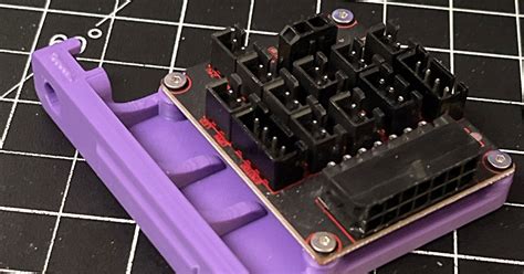
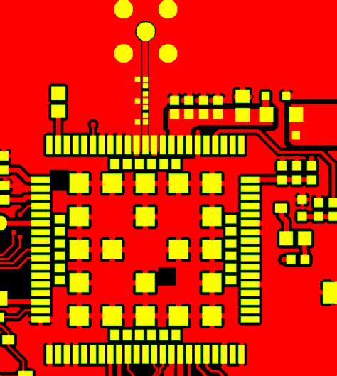
Breakout PCBs are a crucial component in the realm of PCB manufacturing, serving as intermediary boards that facilitate the connection between complex circuit layouts and the pins of surface-mounted devices. These specially designed boards essentially “break out” multiple pads from a single large footprint, allowing for easier access and improved connectivity during the manufacturing process. The primary purpose of breakout PCBs is to ensure that holes and pads are accurately aligned, which in turn enhances solderability and reduces the potential for design flaws during assembly. As you navigate through your own PCB projects, understanding these elements can significantly affect your PCB manufacturing cost. Working with reputable PCB manufacturing companies will also help mitigate risks associated with design errors by providing advanced solutions tailored to your specific needs. In essence, breakout PCBs play a pivotal role in elevating the reliability and efficiency of your electronic designs, guiding you toward successful implementation while minimizing complexities inherent in traditional PCB layouts.
The Importance of Proper Registration in PCB Design
In the realm of PCB manufacturing, ensuring proper registration between holes and pads is paramount. When you focus on accurate alignment, you reduce the risk of design flaws that could cause failure in the final product. The precision in alignment not only enhances solderability but also directly impacts the performance and reliability of your electronic circuits. By prioritizing registration, you can achieve optimal conductivity and minimize the potential for unnecessary electrical resistance. Additionally, PCB manufacturing companies often emphasize this aspect during their processes, as it leads to higher-quality boards and reduced assembly issues. Consider the overall impact on your PCB manufacturing cost; investing time in ensuring proper registration can save money long term by avoiding costly reworks and failures. A well-designed layout, coupled with effective registration practices, is critical for anyone running a PCB manufacturing business, as it lays the foundation for successful project outcomes. Utilizing reliable resources like Andwin PCB can also provide further insights into best practices and technologies that support accurate registration throughout production.
Understanding Annular Rings: Solderability and Performance
When it comes to PCB manufacturing, understanding the role of annular rings is essential for achieving optimal solderability and performance in your designs. An annular ring surrounds a hole in a PCB and acts as a critical interface between the pad and the hole. If the size of these rings is not carefully calculated during the design phase, it can lead to misalignment issues that might affect the electrical performance of your circuit. This is particularly crucial when you consider that most PCB manufacturing companies require precise dimensions to maintain quality throughout production. Inadequate annular rings can hinder effective soldering; thus, when you are preparing your designs, ensure that these rings are not only appropriately sized but also placed correctly relative to vias and pads. This attention to detail can significantly reduce your PCB manufacturing cost as it minimizes potential rework due to design flaws or soldering issues. Staying informed about best practices in annular ring design thereby enhances both functionality and reliability in your PCB projects, ultimately benefiting your PCB manufacturing business overall. Understanding these aspects will not only save you time during the assembly process but also contribute to a higher-quality finished product that meets industry standards.
Common Challenges with Breakout PCBs and Solutions
When working with breakout PCBs, you may encounter several common challenges that can impact the efficiency and effectiveness of your designs. One prevalent issue is achieving proper registration between holes and pads. Misalignment can lead to poor solderability, increasing the risk of connection failures. To mitigate this, consider investing time into precise alignment during the PCB manufacturing process to ensure that all components fit correctly. Another challenge is dealing with the pcb manufacturing cost, especially if multiple iterations are necessary to perfect a design. In such cases, collaborating with reputable pcb manufacturing companies that offer competitive pricing can help you manage expenses while maintaining quality. Additionally, you might face circuit design flaws stemming from insufficient annular rings, which are crucial for reliable solder joints. To avoid this, be diligent in your design phase; ensure that your layout accommodates sufficient space for these rings without compromising component placement.
Lastly, employing simulation tools before actual manufacturing can save both time and resources by identifying potential issues early on in the development of your pcb manufacturing business. By understanding these challenges and proactively addressing them, you can enhance the performance of your breakout circuits and lead successful projects.
Best Practices for Designing Breakout Circuits
When it comes to designing breakout circuits, adhering to best practices can significantly enhance the performance and reliability of your electronic designs. First, ensure that the registration between holes and pads is precise, as inaccuracies can result in soldering issues that affect the overall functionality of the PCB. Incorporating proper trace widths is another crucial factor; you should calculate this based on the current your components will carry, which in turn influences the overall PCB manufacturing cost. By working closely with reputable PCB manufacturing companies, you can obtain valuable feedback on design adjustments before moving into production.
Additionally, maintaining a clear balance between component density and trace routing is vital. Using design rule checks (DRCs) throughout your design workflow helps catch potential problems early on. Pay careful attention to clearance specifications, particularly around vias that connect to multiple layers of a panel; inadequate spacing can lead to failures during soldering or operational use. Lastly, it’s worth noting that investing in advanced simulation tools will allow you to anticipate potential issues and streamline the pcb manufacturing process, ultimately benefiting your pcb manufacturing business.
“A well-designed breakout circuit not only improves solderability but also optimizes signal integrity and reduces overall production headaches.” Remember, thorough preparation can save you time and resources when dealing with eventual design iterations during the pcb manufacturing phase.
Case Studies: Effective Use of Breakout PCBs in Projects
In the world of PCB manufacturing, the strategic implementation of breakout PCBs can greatly enhance project outcomes. For instance, consider a project where a startup aimed to develop a compact wearable device. The team faced challenges with tight space constraints and a complex arrangement of components. By meticulously designing breakout circuits, they ensured that every pad and hole was properly registered, which significantly improved the overall solderability and reduced the risk of defects. Another example involves a telecommunications company that needed to increase the reliability of its signal processing unit. By using advanced PCBs with well-designed breakout layouts and optimal annular rings, they could minimize interference and enhance performance across their network systems. These projects underscore the importance of choosing reputable PCB manufacturing companies that understand how to effectively integrate breakout strategies while keeping an eye on overall manufacturing costs. Ultimately, these real-world applications illustrate how embracing innovative designs in breakout PCB circuits not only addresses common engineering challenges but also contributes to a successful pcb manufacturing business by delivering high-quality, reliable electronic products.
Future Trends in PCB Design and Technology
As the landscape of PCB design and technology continues to evolve, industry stakeholders are increasingly focused on optimizing the pcb manufacturing process to meet the rising demand for efficiency and functionality. One noticeable trend is the integration of advanced materials that not only enhance performance but also reduce pcb manufacturing costs. Companies are exploring innovations in substrates that offer improved thermal management and signal integrity, which are crucial for high-frequency applications. Additionally, automation and digitalization are becoming commonplace within pcb manufacturing companies, aiming to streamline production processes and minimize human error. This shift towards automation aids in faster prototype developments while allowing designers to allocate resources more effectively. The emergence of specialized software tools that simulate real-world conditions during the design phase is also notable; these tools facilitate better decision-making and reduce the likelihood of encountering significant design flaws later on. Overall, the future outlook for pcb manufacturing is geared toward creating more reliable, cost-effective solutions that meet the challenges posed by contemporary electronic applications while ensuring optimal performance throughout their lifecycle.
Conclusion
In summary, understanding the role of breakout PCBs is essential in the realm of PCB manufacturing. These specialized designs not only enable smooth transitions and connections between various components but also uphold the integrity of your overall circuit. As you navigate through pcb manufacturing cost considerations, it’s crucial to remember that investing in quality design can mitigate potential issues related to alignment and solderability. This, in turn, can significantly impact the reliability and performance of your projects. Partnering with reputable pcb manufacturing companies can provide valuable insights into best practices and help you avoid common pitfalls associated with breakout designs. Additionally, acknowledging the nuances of pcb manufacturing business, such as efficient supply chain management and advanced technology adoption, will ensure that your circuit designs are not just functional but also economically viable. In conclusion, a meticulous approach to designing breakout PCBs will pave the way for durable and effective electronic solutions in your endeavors.
FAQs
What is a breakout PCB and why is it used?
A breakout PCB is a type of printed circuit board (PCB) designed to take connections from a larger component and distribute them to smaller, more manageable pads. This helps enhance the electrical connections in your design and is critical for ensuring proper registration between holes and pads.
How do I choose the right PCB manufacturing companies?
When choosing PCB manufacturing companies, consider their experience, customer reviews, technology capabilities, and compatibility with your specific design requirements. Ensure they understand the nuances of breakout PCBs to facilitate better performance.
What factors influence the PCB manufacturing cost?
The PCB manufacturing cost typically depends on several factors, including material type, board complexity, layer count, and lead time. Incorporating effective breakout designs can help streamline production and potentially lower costs.
Can I integrate breakout PCBs into my current PCB manufacturing business?
Yes, integrating breakout PCBs into your existing processes can improve efficiency—especially if you’re looking to enhance solderability and minimize design flaws in your electronic circuits. It also opens up opportunities for more complex designs that meet modern requirements.
What are common issues faced with breakout PCBs during PCB manufacturing?
Common issues include misalignments between pads and holes, which can lead to poor solder joints. Addressing these challenges early in the design phase can mitigate costly errors during PCB manufacturing, saving time and resources.
If you are interested in learning more about effective PCB manufacturing, please click here: Learn More About PCB Manufacturing.