Understanding Printed Circuit Board and Assembly Processes
Key Takeaways
When delving into the world of printed circuit board assembly (PCBA), several key points stand out that are essential for anyone involved in this critical aspect of electronics manufacturing. Understanding the fundamentals of PCB design and assembly is paramount; it allows manufacturers to create reliable products that meet rigorous performance standards. The PCB serves as the backbone of electronic devices, providing a platform for both passive and active components.
One of the crucial aspects to keep in mind is the variety of materials utilized in PCB production, which can significantly influence both functionality and durability. Choices range from various types of copper, used for conductive pathways, to insulating substrates like FR-4, a commonly used fiberglass material. Additionally, advancements in assembly techniques such as surface mount technology (SMT) and through-hole connections enhance both speed and precision during production.
To ensure the success of a pcba, implementing best practices is vital. This includes maintaining strict quality control measures throughout both the design and assembly phases to prevent common PCB issues such as misalignment or solder defects. A well-organized workflow not only boosts efficiency but also improves overall product reliability.
For those aiming to stay ahead in this dynamic field, being aware of emerging trends—such as increased automation in PCB manufacturing—can offer significant advantages. These trends not only optimize processes but also promise higher quality and lower costs, paving the way for even more innovative electronic designs.
In summary, a comprehensive understanding of these elements can lead to more effective strategies in creating high-quality PCBs and assemblies that meet market demands.
| Aspect | Importance |
|---|---|
| Material Selection | Affects performance and durability |
| Assembly Techniques | Enhances precision during production |
| Quality Control Practices | Prevents defects and ensures reliability |
| Awareness of Trends | Enables adaptation to market demands |
Introduction to Printed Circuit Boards: An Overview
Printed Circuit Boards (PCBs) are crucial components in nearly all electronic devices, serving as the foundation for electrical connections and signal transmission. The pcb assembly process transforms intricate designs into functional hardware, ensuring the reliability and performance of electronic systems. At their core, PCBs consist of conductive paths that connect various key components, such as resistors, capacitors, and microchips, enabling them to work in tandem.
Understanding the layout and design principles is essential for anyone involved in electronics or engineering. The transition from design to physical board involves meticulous planning and execution. Techniques such as surface mount technology (SMT) and through-hole assembly are vital for effective pcba processes. Each method has its strengths; for instance, SMT is favored for high-density applications and smaller components, optimizing space and functionality.
Moreover, selecting appropriate materials is essential to optimize the performance of PCBs under varied conditions. For example, the choice of substrate material affects not only the electrical characteristics but also thermal management during use. Therefore, thorough knowledge of both the mechanical properties and thermal conductivity requirements can significantly enhance the durability and efficiency of pcba.
“Efficient pcb assembly requires a comprehensive understanding of the entire lifecycle from design to final testing.”
By focusing on these fundamental aspects, professionals can ensure high-quality production while minimizing common pitfalls associated with PCB fabrication and assembly. Understanding these principles lays a solid foundation for mastering more advanced techniques prevalent in today’s rapidly evolving electronic landscape.
Key Components of PCB Design
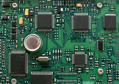
The design of a printed circuit board (PCB) is a complex process that involves multiple key components, each crucial for the overall functionality and reliability of the final product. One of the primary elements is the layout, which determines the arrangement of electronic components and their respective connections. A well-thought-out layout not only enhances performance but also simplifies pcb assembly processes, allowing for efficient integration during manufacturing. Another significant factor is the selection of materials; high-quality substrates and conductive elements ensure optimal conductivity and durability, directly impacting the effectiveness of the pcba. Furthermore, design rules such as spacing and trace width must be adhered to in order to prevent issues like signal interference or thermal overstress. Additionally, considerations around thermal management are critical, as PCBs must dissipate heat effectively to maintain operational integrity. Understanding these components allows designers to create PCBs that not only meet technical specifications but are also suited for scalable production processes in high-quality electronic components. Each decision made during this phase influences both manufacturing efficiency and product reliability in the competitive electronics market.
PCB Manufacturing Processes Explained
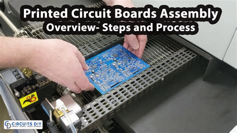
The manufacturing of printed circuit boards (PCBs) involves a series of intricate processes that ensure the final product meets the necessary specifications for functionality and reliability. Initially, PCB design is meticulously planned, focusing on the layout of electrical pathways and component placement. Once the design is finalized, it transitions to the fabrication stage, where various materials such as copper foil, substrates, and laminates are utilized to create the circuit board. The process involves etching away unwanted copper using chemical processes to form conductive pathways. Subsequently, drilling holes for component placement is crucial in facilitating connections.
Assembling these components onto the board constitutes a vital phase known as PCB assembly (PCBA). During this stage, techniques such as surface-mount technology (SMT) and through-hole mounting are employed to position electrical components accurately on the PCB. Each method has its advantages; for instance, SMT allows for higher density placement of components, which is essential for modern compact designs.
To ensure the production of high-quality PCBs, rigorous testing processes are implemented throughout manufacturing. These tests check for structural integrity and electrical performance, identifying any potential issues before they reach end-users. Thus, understanding these essential manufacturing processes not only aids in better product development but also contributes significantly to the reliability and efficiency of electronic devices in various applications.
Assembly Techniques for High-Quality PCBs
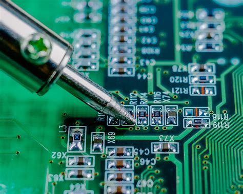
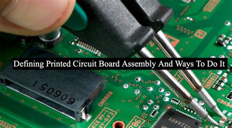
The process of pcb assembly is crucial in ensuring that electronic devices function reliably and efficiently. Various assembly techniques are employed to achieve high-quality PCBAs (Printed Circuit Board Assemblies), each serving specific purposes depending on the complexity and requirements of the design. One popular method is Surface Mount Technology (SMT), which involves placing components directly onto the surface of the PCB, allowing for a more compact design and improved performance. Conversely, Through-Hole Technology (THT) remains relevant for larger components and offers greater mechanical strength, particularly in demanding applications.
To further enhance the quality of pcba, proper soldering techniques must be employed, with choices such as manual soldering or automated processes like wave soldering or reflow soldering. The use of appropriate solder materials also plays a critical role; lead-free solders are increasingly becoming favored due to environmental considerations and compliance with global standards. Additionally, ensuring an optimal thermal profile during soldering processes minimizes defects and enhances component reliability.
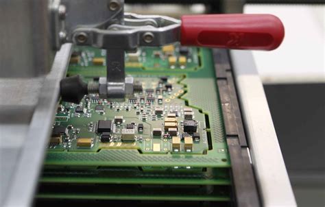
Another important aspect of pcb assembly is the use of advanced inspection techniques such as Automated Optical Inspection (AOI) to catch potential issues early. Visual checks or x-ray inspection may also be necessary for hidden joints after assembly. By implementing these techniques diligently, manufacturers can significantly reduce the likelihood of defects in their final products, leading to increased customer satisfaction and reduced warranty claims.
In summary, mastering different assembly techniques is essential for producing high-quality PCBAs, emphasizing the right methodologies and adherence to established best practices to foster reliability in electronic applications.
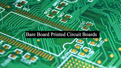
Materials Used in PCB Production
The selection of materials for printed circuit board (PCB) production is crucial in determining the overall performance and reliability of electronic devices. The base material, often composed of epoxy glass, plays a significant role in the structure of the PCB, providing durability and insulation. Common choices include FR-4, which is favored for its excellent electrical properties, and polyimide, which offers superior thermal resistance for high-temperature applications. Additionally, conducting materials such as copper are essential for creating pathways that support electrical signals within the circuit. In PCB assembly (pcba), soldering materials like lead-free solder have gained popularity for their environmentally friendly characteristics, ensuring that the assembly process adheres to modern regulatory standards. Furthermore, dielectric materials are employed to isolate conductive layers effectively while maintaining signal integrity. Selecting appropriate materials not only enhances the efficiency of pcb assembly, but also contributes to the longevity and functionality of electronic components, making material choices a vital aspect in achieving high-quality PCBs.
Best Practices for Efficient PCB Assembly
Achieving an efficient PCB assembly (PCBA) process is essential for producing high-quality electronic components. One of the primary best practices involves meticulously planning the layout of the printed circuit board. Ensuring that components are arranged logically not only speeds up the assembly process but also minimizes the risk of errors. Furthermore, utilizing standardized components can significantly enhance efficiency, as familiar parts streamline both assembly and maintenance. Additionally, investing in automated machinery can dramatically reduce manual labor and increase precision during the PCBA process.
Careful selection of solder materials is another crucial aspect; using lead-free solder can improve reliability while also adhering to environmental regulations. Regular quality control checks throughout the assembly stages are vital to identify defects early, thus avoiding costly rework or production delays. Moreover, implementing a robust feedback loop with the design team facilitates continuous improvement in PCB assembly practices. Overall, by prioritizing these best practices, manufacturers can not only improve efficiency in their PCBA processes but also ensure consistent quality in their electronic products.
Troubleshooting Common PCB Issues
In the realm of PCB assembly or PCBA, encountering issues during production is a common challenge that can affect the overall quality of the electronic components. Identifying these problems early is essential for maintaining efficiency and ensuring product reliability. One prevalent issue is solder bridging, which occurs when solder mistakenly connects two or more pads, causing short circuits. To mitigate this, careful inspection of the solder paste application and pick-and-place processes is crucial. Another potential problem is delamination, where the layers of the printed circuit board separate due to heat or moisture exposure, leading to performance failures over time. Employing high-quality materials and ensuring proper environmental controls during assembly can help prevent this issue.
Additionally, misaligned components during PCBA can cause malfunctioning circuits. Employing precise alignment technology and double-checking component placement before soldering are key strategies to avoid this pitfall. Lastly, thermal stress can impact solder joints and circuit integrity; thus, implementing controlled thermal management practices throughout both design and manufacturing phases is vital for sustaining the longevity of your PCB products. By addressing these common issues with vigilance and employing best practices in PCB assembly, quality standards can be upheld effectively, ensuring robust performance in electronic applications.
Future Trends in PCB Design and Assembly
As technology continues to evolve, the landscape of printed circuit board (PCB) design and assembly (PCBA) is expected to undergo significant transformations. One of the most notable trends is the increasing miniaturization of electronic components, which demands innovative PCB layouts that maximize space while maintaining functionality. Concurrently, advanced materials, such as flexible and high-frequency laminates, are being integrated into PCBA processes to enhance performance and reliability. The rise of automation in the assembly processes further accelerates production efficiency and precision through techniques like robotic soldering and automated optical inspection. Additionally, sustainability is becoming a key focus, with manufacturers exploring eco-friendly materials and practices in their PCB assembly operations to minimize waste and reduce environmental impact. The adoption of Internet of Things (IoT) technologies also plays a crucial role, allowing for smarter devices connected through robust PCBs designed for varied applications. As these trends unfold, staying informed about innovations will be vital for industry stakeholders aiming to optimize their printed circuit board designs and assembly processes while maintaining high quality standards.
Conclusion
In summary, the journey of designing and producing printed circuit boards (PCBs) is a complex yet fascinating process that directly impacts the efficiency and functionality of electronic devices. The intersection of PCB design and assembly, commonly referred to as PCB assembly (PCBA), exemplifies a critical phase where precision meets innovation. To achieve a superior pcba outcome, understanding the comprehensive approach to both design and manufacturing processes is imperative. Emphasizing quality materials, skilled labor, and state-of-the-art assembly techniques will ensure that the final product meets stringent electronic standards. Continuous improvements in technology are shaping the future of PCB production; therefore, staying updated with emerging trends can provide significant advantages in this competitive industry. Effective troubleshooting mechanisms also play an essential role in maintaining production quality and minimizing errors during both the design and assembly phases. As manufacturers navigate this evolving landscape, fostering an environment where best practices are routinely applied will help in achieving high-quality electronic components that perform reliably over time.
FAQs
What is PCB assembly?
PCB assembly, or PCBA, refers to the process of soldering electronic components to a printed circuit board, creating a functional electronic circuit.
What are the key steps involved in the PCB assembly process?
The key steps in PCB assembly include design, printing the circuit board, mounting components, soldering, and testing the final product to ensure quality and functionality.
What materials are commonly used in PCB assembly?
Common materials for PCBA include copper for traces, various substrates like FR-4 or polyimide for boards, and solder paste or adhesives for mounting components.
How do I ensure high-quality PCBs during assembly?
To ensure high-quality PCBs, it is essential to use reliable components, maintain strict quality control throughout the manufacturing process, and follow best practices during assembly.
What are some common issues faced in PCB assembly?
Common issues include misalignment of components, cold solder joints, insufficient soldering, or contamination on the board that affects connection quality.