Fr4 pcb manufacturing process
Understanding The Basics Of FR4 Material In PCB Manufacturing
In the realm of printed circuit board (PCB) manufacturing, the choice of substrate material is crucial to the performance and reliability of the final product. One of the most commonly used materials in this industry is FR4, a composite material that serves as the backbone for a wide array of electronic devices. Understanding the basics of FR4 material in PCB manufacturing is essential for anyone involved in the design and production of electronic circuits.
FR4 is a grade designation for flame-retardant fiberglass-reinforced epoxy laminate.
The “FR” stands for “flame retardant,” while the “4” indicates a specific grade within the NEMA (National Electrical Manufacturers Association) standards. This material is renowned for its excellent balance of mechanical strength, electrical insulation properties, and thermal resistance, making it an ideal choice for a variety of applications. The core of FR4 is composed of woven fiberglass cloth, which is then impregnated with an epoxy resin binder. This combination results in a material that is not only robust but also lightweight, providing a stable platform for the intricate copper traces that form the circuitry of a PCB.
The manufacturing process of FR4-based PCBs begins with the preparation of the laminate.
Sheets of FR4 are cut to the desired size, and copper foil is laminated onto one or both sides of the substrate. This copper layer is essential, as it will be etched away to create the circuit patterns. The next step involves the application of a photosensitive resist to the copper surface. This resist is then exposed to ultraviolet light through a photomask, which contains the desired circuit pattern. The areas of the resist exposed to the light harden, while the unexposed areas remain soft and are subsequently washed away, revealing the underlying copper.
Following this, the PCB undergoes an etching process, typically using a chemical solution such as ferric chloride or ammonium persulfate.
This solution removes the unwanted copper, leaving behind only the circuit pattern protected by the hardened resist. Once the etching is complete, the remaining resist is stripped away, exposing the clean copper traces. At this stage, the PCB may undergo additional processes such as drilling, where holes are created for component leads and vias, and plating, where these holes are coated with copper to ensure electrical connectivity between different layers of the board.
The final steps in the FR4 PCB manufacturing process include solder mask application and silkscreen printing.
The solder mask, usually green in color, is applied to protect the copper traces from oxidation and to prevent solder bridges during component assembly. The silkscreen layer provides labels and markings that assist in the assembly and testing of the PCB. Quality control measures are implemented throughout the manufacturing process to ensure that the final product meets the required specifications and performance standards.
In conclusion, FR4 material plays a pivotal role in PCB manufacturing due to its favorable properties and versatility. Its ability to provide a reliable and durable platform for electronic circuits makes it a preferred choice in the industry. Understanding the intricacies of FR4 and its manufacturing process is fundamental for producing high-quality PCBs that meet the demands of modern electronic applications. As technology continues to evolve, the importance of materials like FR4 in the development of innovative electronic solutions remains ever significant.

Step-By-Step Guide To The FR4 PCB Fabrication Process
The fabrication of FR4 PCBs, or printed circuit boards, is a meticulous process that involves several critical steps to ensure the final product meets the required specifications and performance standards.
FR4, a composite material made from woven fiberglass cloth with an epoxy resin binder, is renowned for its excellent strength-to-weight ratio and electrical insulation properties, making it a popular choice in the electronics industry. Understanding the step-by-step process of FR4 PCB manufacturing is essential for anyone involved in electronics design and production.
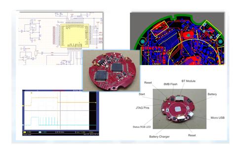
The journey begins with the design phase, where engineers use specialized software to create a detailed schematic of the circuit.
This schematic is then translated into a layout that specifies the exact placement of components and the routing of electrical connections. Once the design is finalized, it is converted into a format suitable for manufacturing, typically Gerber files, which contain all the necessary information for each layer of the PCB.
Following the design phase, the manufacturing process commences with the preparation of the FR4 substrate.
The substrate is cut into panels of the desired size, and a thin layer of copper is laminated onto one or both sides, depending on whether a single or double-sided PCB is being produced. This copper layer will form the conductive pathways of the circuit.
The next step is the application of a photosensitive resist to the copper-clad panels.
This resist is crucial for the subsequent photolithography process, where the PCB design is transferred onto the substrate. The panels are exposed to ultraviolet light through a photomask that contains the circuit pattern. The areas exposed to light harden, while the unexposed areas remain soft and are subsequently washed away, revealing the copper beneath.
With the circuit pattern now visible, the panels undergo an etching process to remove the unwanted copper.
This is typically achieved using a chemical solution that dissolves the exposed copper, leaving only the desired circuit traces intact. After etching, the remaining photoresist is stripped away, exposing the clean copper traces.
To ensure electrical connectivity between different layers of a multi-layer PCB, holes are drilled at precise locations.
These holes, known as vias, are then plated with copper to establish electrical connections between the layers. The drilling process requires high precision to avoid damaging the delicate circuit traces.
Once the vias are plated, the PCB undergoes a solder mask application.
The solder mask is a protective layer that prevents solder bridges and short circuits during component assembly. It also provides a degree of environmental protection to the copper traces. The solder mask is typically green, although other colors are available.
The final step in the fabrication process is the application of a surface finish, which protects the exposed copper pads and facilitates soldering during assembly. Common finishes include HASL (Hot Air Solder Leveling), ENIG (Electroless Nickel Immersion Gold), and OSP (Organic Solderability Preservative), each offering distinct advantages depending on the application.
In conclusion, the FR4 PCB manufacturing process is a complex sequence of steps that transforms a conceptual design into a functional electronic component. Each stage, from design to surface finishing, requires precision and attention to detail to ensure the final product meets the stringent demands of modern electronics. Understanding this process is crucial for engineers and manufacturers striving to produce high-quality PCBs that power the devices of today and tomorrow.

Key Advantages Of Using FR4 In PCB Production
FR4, a widely recognized material in the realm of printed circuit board (PCB) manufacturing, offers a multitude of advantages that make it a preferred choice for many electronic applications. As the backbone of modern electronics, PCBs require materials that not only support the intricate circuitry but also ensure reliability and performance. FR4, a composite material made from woven fiberglass cloth with an epoxy resin binder, excels in meeting these requirements, thus playing a crucial role in the production of high-quality PCBs.
One of the primary advantages of using FR4 in PCB production is its excellent electrical insulation properties.
This material is renowned for its ability to maintain electrical insulation even in high humidity environments, which is essential for the stability and performance of electronic devices. The dielectric properties of FR4 ensure that the electrical signals within the PCB are transmitted with minimal loss, thereby enhancing the overall efficiency of the device. Furthermore, FR4’s ability to withstand high voltages without breaking down makes it an ideal choice for a wide range of applications, from consumer electronics to industrial machinery.
In addition to its electrical properties, FR4 is highly valued for its mechanical strength.
The fiberglass reinforcement provides a robust structure that can withstand physical stress and mechanical shock. This durability is particularly important in applications where the PCB may be subjected to rough handling or extreme conditions. The rigidity of FR4 ensures that the PCB maintains its shape and integrity, preventing damage to the delicate circuitry embedded within. Consequently, this mechanical resilience contributes to the longevity and reliability of electronic devices, reducing the need for frequent repairs or replacements.
Another significant advantage of FR4 is its thermal stability.
Electronic devices often generate heat during operation, and it is crucial for the PCB material to withstand these temperatures without degrading. FR4 exhibits excellent thermal resistance, maintaining its properties across a wide temperature range. This characteristic not only prevents the material from warping or melting but also protects the components mounted on the PCB from heat-related damage. As a result, FR4-based PCBs are suitable for use in environments where temperature fluctuations are common, ensuring consistent performance and reliability.
Moreover, FR4 is a cost-effective material, which is a critical consideration in the competitive electronics industry.
Its widespread availability and ease of manufacturing contribute to lower production costs, making it an economical choice for both small-scale and large-scale PCB production. The cost-effectiveness of FR4 does not compromise its quality, as it continues to deliver exceptional performance across various applications. This balance of affordability and functionality makes FR4 an attractive option for manufacturers seeking to optimize their production processes without sacrificing quality.
In conclusion, the use of FR4 in PCB manufacturing offers numerous advantages that enhance the performance, durability, and cost-effectiveness of electronic devices. Its superior electrical insulation, mechanical strength, thermal stability, and affordability make it an indispensable material in the electronics industry. As technology continues to evolve, the demand for reliable and efficient PCBs will only increase, further solidifying FR4’s position as a cornerstone in the production of cutting-edge electronic solutions.

Common Challenges And Solutions In FR4 PCB Manufacturing
In the realm of electronics, the manufacturing of FR4 printed circuit boards (PCBs) is a critical process that underpins the functionality of countless devices. However, this process is not without its challenges. Understanding these challenges and their corresponding solutions is essential for manufacturers aiming to produce high-quality PCBs efficiently and cost-effectively.
One of the primary challenges in FR4 PCB manufacturing is maintaining dimensional stability
FR4, a composite material made from woven fiberglass cloth with an epoxy resin binder, is known for its excellent mechanical strength and electrical insulation properties. However, it can be susceptible to warping and dimensional changes due to temperature fluctuations during the manufacturing process. To mitigate this issue, manufacturers often employ precise temperature control and use pre-baking techniques to stabilize the material before processing. Additionally, implementing a controlled cooling process can further reduce the risk of warping, ensuring that the final product meets the required specifications.
Another significant challenge is the accurate etching of copper traces on the FR4 substrate.
The etching process involves removing unwanted copper to create the desired circuit pattern. However, achieving precision in this step can be difficult due to factors such as undercutting and over-etching, which can lead to circuit failures. To address this, manufacturers can optimize the etching solution’s concentration and temperature, as well as the duration of the etching process. Employing advanced imaging techniques and automated inspection systems can also enhance accuracy, allowing for early detection and correction of potential defects.
Solder mask application is another area where challenges frequently arise.
The solder mask is a protective layer applied to the PCB to prevent solder bridges and protect against environmental damage. Achieving uniform coverage without defects such as bubbles or pinholes is crucial. To overcome these challenges, manufacturers can utilize high-quality solder mask materials and employ precise application techniques, such as screen printing or spray coating. Additionally, thorough inspection and testing of the solder mask layer can help identify and rectify any inconsistencies before the final assembly.
Thermal management is a further concern in FR4 PCB manufacturing, particularly as electronic devices become more compact and powerful.
Efficient heat dissipation is essential to prevent overheating and ensure the longevity of the device. To address this, manufacturers can incorporate thermal vias, heat sinks, and other thermal management solutions into the PCB design. Moreover, selecting the appropriate thickness and copper weight for the FR4 material can enhance its thermal conductivity, thereby improving overall performance.
Finally, ensuring the reliability and durability of the finished PCB is paramount.
This involves rigorous testing and quality assurance measures throughout the manufacturing process. Implementing automated optical inspection (AOI) and in-circuit testing (ICT) can help identify defects early, reducing the likelihood of failures in the field. Additionally, adhering to industry standards and certifications, such as IPC standards, can provide an extra layer of assurance regarding the quality and reliability of the PCBs produced.
In conclusion, while the manufacturing of FR4 PCBs presents several challenges, a combination of advanced techniques, meticulous process control, and rigorous testing can effectively address these issues. By understanding and implementing these solutions, manufacturers can produce high-quality PCBs that meet the demands of modern electronic applications, ensuring both performance and reliability.


