Hdi in pcb design
Importance Of HDI In Modern PCB Design
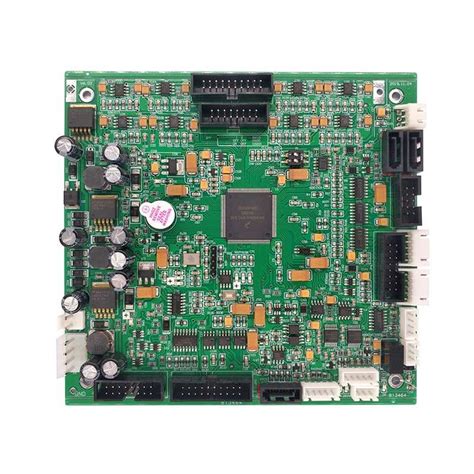
High-Density Interconnect (HDI) technology has become a cornerstone in modern printed circuit board (PCB) design, playing a pivotal role in the advancement of electronic devices. As the demand for more compact, efficient, and powerful electronic products continues to rise, the importance of HDI in PCB design cannot be overstated. This technology enables the creation of smaller, lighter, and more efficient PCBs, which are essential for the development of contemporary electronic devices such as smartphones, tablets, and wearable technology.
One of the primary reasons HDI is crucial in modern PCB design is its ability to support miniaturization.
As electronic devices become increasingly compact, the need for smaller components and more efficient use of space on PCBs becomes paramount. HDI technology allows for the integration of more components in a smaller area by utilizing finer lines and spaces, smaller vias, and higher connection pad density. This results in a significant reduction in the overall size and weight of the PCB, which is essential for portable and wearable devices where space is at a premium.
Moreover, HDI technology enhances the performance and reliability of PCBs.
By enabling shorter signal paths and reducing the number of layers required, HDI designs can improve signal integrity and reduce electromagnetic interference. This is particularly important in high-speed and high-frequency applications where signal quality is critical. Additionally, the use of microvias in HDI designs allows for better thermal management, which is crucial for maintaining the performance and longevity of electronic components.
Transitioning to another significant aspect, HDI technology also facilitates the integration of advanced features and functionalities in electronic devices.
As consumer expectations continue to evolve, there is a growing demand for devices that offer more features without compromising on size or performance. HDI PCBs can accommodate complex circuitry and support the integration of advanced technologies such as 5G, IoT, and AI, enabling manufacturers to meet these demands. This capability is essential for staying competitive in the fast-paced electronics market.
Furthermore, the use of HDI in PCB design contributes to cost efficiency in the manufacturing process.
Although the initial design and fabrication of HDI PCBs may be more expensive than traditional PCBs, the long-term benefits often outweigh these costs. The reduction in size and weight can lead to lower material costs and reduced shipping expenses. Additionally, the improved performance and reliability of HDI PCBs can result in fewer defects and returns, ultimately saving manufacturers money.
In conclusion, the importance of HDI in modern PCB design is evident in its ability to support the miniaturization of electronic devices, enhance performance and reliability, enable the integration of advanced features, and contribute to cost efficiency. As technology continues to evolve, the role of HDI in PCB design will only become more critical. Manufacturers and designers must continue to embrace and innovate with HDI technology to meet the ever-growing demands of the electronics industry. By doing so, they can ensure that their products remain at the forefront of technological advancement, offering consumers the cutting-edge features and performance they expect in today’s digital age.
Key Benefits Of Implementing HDI Technology
High-Density Interconnect (HDI) technology has emerged as a pivotal advancement in the field of printed circuit board (PCB) design, offering a multitude of benefits that significantly enhance the performance and capabilities of electronic devices. As the demand for more compact, efficient, and powerful electronic products continues to rise, HDI technology provides a solution that meets these requirements by enabling the design of smaller, faster, and more efficient PCBs.
One of the primary benefits of implementing HDI technology in PCB design is the ability to achieve higher component density.
HDI PCBs utilize finer lines and spaces, smaller vias, and capture pads, which allow for more components to be placed on a single board. This increased density is crucial for modern electronic devices, which are continually being miniaturized to meet consumer demand for portability and convenience. By enabling more components to fit into a smaller area, HDI technology supports the development of compact devices without compromising on functionality or performance.
In addition to higher component density, HDI technology enhances signal integrity, which is a critical factor in the performance of electronic devices.
The shorter distances between components on an HDI PCB reduce the time it takes for signals to travel, thereby minimizing signal loss and improving overall signal quality. This is particularly important in high-speed applications where maintaining signal integrity is essential for reliable device operation. Furthermore, the use of microvias in HDI designs helps to reduce parasitic capacitance and inductance, further contributing to improved signal performance.
Another significant advantage of HDI technology is its contribution to improved thermal management.
As electronic devices become more powerful, they generate more heat, which can adversely affect performance and reliability. HDI PCBs are designed to efficiently dissipate heat, thanks to their layered construction and the use of advanced materials. This effective thermal management ensures that devices operate within safe temperature ranges, thereby enhancing their longevity and reliability.
Moreover, HDI technology facilitates the integration of advanced features and functionalities into electronic devices.
The increased routing density and layer count in HDI PCBs allow for the incorporation of complex circuitry and additional features that would be challenging to implement using traditional PCB designs. This capability is particularly beneficial in the development of cutting-edge technologies such as smartphones, tablets, and wearable devices, where space is at a premium, and advanced functionality is a key selling point.
The implementation of HDI technology also leads to cost savings in the long run.
Although the initial design and manufacturing costs of HDI PCBs may be higher compared to traditional PCBs, the benefits of reduced size, improved performance, and enhanced reliability often result in lower overall costs. Devices that are smaller and more efficient require less material and energy to produce and operate, leading to cost efficiencies throughout the product lifecycle.
In conclusion, the adoption of HDI technology in PCB design offers numerous benefits that address the evolving needs of the electronics industry. By enabling higher component density, enhancing signal integrity, improving thermal management, facilitating advanced functionality, and providing cost efficiencies, HDI technology plays a crucial role in the development of modern electronic devices. As technology continues to advance, the importance of HDI in PCB design is likely to grow, making it an indispensable tool for engineers and designers striving to push the boundaries of what is possible in electronic design.
Challenges And Solutions In HDI PCB Manufacturing
High-Density Interconnect (HDI) technology has become a cornerstone in the evolution of printed circuit board (PCB) design, driven by the demand for more compact, efficient, and high-performance electronic devices. However, the manufacturing of HDI PCBs presents a unique set of challenges that require innovative solutions to ensure reliability and functionality. As the industry continues to push the boundaries of miniaturization, understanding these challenges and their corresponding solutions is crucial for manufacturers and designers alike.
One of the primary challenges in HDI PCB manufacturing is the complexity of the design itself.
HDI PCBs are characterized by their use of microvias, finer lines and spaces, and higher layer counts, which allow for increased component density. This complexity necessitates advanced design tools and methodologies to ensure that the intricate layouts are both manufacturable and functional. To address this, manufacturers are increasingly relying on sophisticated computer-aided design (CAD) software that can handle the intricacies of HDI designs, enabling precise control over the placement and routing of components.
Another significant challenge is the material selection for HDI PCBs.
The materials used must not only support the high-density interconnections but also withstand the thermal and mechanical stresses encountered during operation. Traditional materials may not suffice, leading to the adoption of advanced laminates and substrates that offer superior thermal management and mechanical stability. These materials, however, can be more expensive and difficult to source, necessitating a careful balance between performance requirements and cost considerations.
The manufacturing process itself poses additional challenges, particularly in the drilling and plating of microvias.
Microvias, which are essential for the high-density interconnections in HDI PCBs, require precise drilling techniques to ensure their integrity and reliability. Laser drilling has emerged as a preferred method due to its precision and ability to create small, clean holes. However, this technique demands significant investment in specialized equipment and expertise. Furthermore, the plating process for these microvias must be meticulously controlled to ensure proper conductivity and adhesion, often requiring advanced plating chemistries and processes.
Signal integrity is another critical concern in HDI PCB manufacturing.
As the density of interconnections increases, so does the potential for signal interference and loss. To mitigate these issues, designers must employ advanced signal integrity analysis tools and techniques during the design phase. This includes careful consideration of trace impedance, crosstalk, and electromagnetic interference (EMI), which can be addressed through strategic layer stacking, controlled impedance routing, and the use of shielding materials.
Despite these challenges, the solutions being developed are paving the way for more robust and efficient HDI PCB manufacturing processes.
Collaboration between designers, material scientists, and manufacturers is essential to overcome these hurdles and drive innovation in the field. By leveraging advanced technologies and methodologies, the industry can continue to meet the growing demand for high-performance electronic devices.
In conclusion, while HDI PCB manufacturing presents a range of challenges, the solutions being implemented are enabling the production of increasingly sophisticated and reliable PCBs. As technology continues to advance, the industry must remain agile and adaptive, embracing new tools and techniques to address the evolving demands of HDI design and manufacturing. Through continued innovation and collaboration, the potential of HDI technology can be fully realized, leading to the next generation of electronic devices.
Future Trends In HDI PCB Design And Applications
High-Density Interconnect (HDI) technology has become a cornerstone in the evolution of printed circuit board (PCB) design, driven by the relentless demand for miniaturization and enhanced performance in electronic devices. As we look to the future, several trends are poised to shape the landscape of HDI PCB design and its applications, promising to push the boundaries of what is currently possible.
To begin with, the increasing complexity of electronic devices necessitates more sophisticated HDI designs.
The proliferation of Internet of Things (IoT) devices, wearable technology, and advanced communication systems requires PCBs that can accommodate a higher number of components in a smaller area. This demand is leading to the development of multi-layer HDI PCBs, which allow for more interconnections and components without increasing the board’s size. Consequently, designers are focusing on optimizing layer stack-ups and employing advanced via technologies, such as microvias and blind/buried vias, to enhance connectivity and performance.
Moreover, the integration of advanced materials is another trend that is gaining momentum in HDI PCB design.
Traditional materials like FR-4 are being supplemented or replaced by high-performance substrates that offer better thermal management, signal integrity, and mechanical strength. Materials such as liquid crystal polymer (LCP) and polytetrafluoroethylene (PTFE) are becoming more prevalent, especially in applications requiring high-frequency performance, such as 5G networks and radar systems. These materials not only support the miniaturization trend but also improve the overall reliability and efficiency of the PCBs.
In addition to material advancements, the adoption of automation and artificial intelligence (AI) in the design and manufacturing processes is revolutionizing HDI PCB production.
AI-driven design tools are enabling engineers to optimize layouts more efficiently, predict potential design flaws, and reduce time-to-market. Automation in manufacturing, on the other hand, ensures precision and consistency, which are critical in producing the intricate features of HDI PCBs. This technological synergy is expected to enhance the scalability and cost-effectiveness of HDI solutions, making them more accessible for a broader range of applications.
Furthermore, the push towards sustainability is influencing HDI PCB design.
As environmental concerns become more pressing, there is a growing emphasis on developing eco-friendly manufacturing processes and materials. This includes reducing the use of hazardous substances, improving energy efficiency during production, and designing for recyclability. The industry is also exploring the use of biodegradable materials and innovative recycling techniques to minimize the environmental impact of electronic waste.
Finally, the future of HDI PCB applications is expanding beyond traditional consumer electronics.
The automotive industry, for instance, is increasingly adopting HDI technology to support the development of advanced driver-assistance systems (ADAS) and electric vehicles (EVs). Similarly, the medical field is leveraging HDI PCBs for compact and reliable medical devices, such as implantable sensors and portable diagnostic tools. These emerging applications underscore the versatility and critical role of HDI technology in driving innovation across various sectors.
In conclusion, the future of HDI PCB design and applications is characterized by a confluence of technological advancements, material innovations, and a commitment to sustainability. As these trends continue to evolve, they will undoubtedly redefine the capabilities and applications of HDI technology, paving the way for a new era of electronic design and functionality.