Hdi pcb 2+4+2
Advantages Of HDI PCB 2+4+2 Design
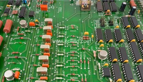
The HDI PCB 2+4+2 design represents a significant advancement in the field of printed circuit board technology, offering numerous advantages that cater to the ever-evolving demands of modern electronic devices.
As electronic components continue to shrink in size while increasing in functionality, the need for more sophisticated and efficient PCB designs has become paramount. The HDI PCB 2+4+2 design, characterized by its high-density interconnect structure, addresses these needs by providing a compact yet highly functional solution.
One of the primary advantages of the HDI PCB 2+4+2 design is its ability to support higher component density.
This design incorporates multiple layers, specifically two outer layers, four inner layers, and two additional layers, which allow for a greater number of interconnections within a limited space. Consequently, this increased density enables the integration of more components on a single board, which is particularly beneficial for devices that require complex circuitry in a compact form factor. This capability is crucial for industries such as consumer electronics, telecommunications, and automotive, where space constraints are a constant challenge.
Moreover, the HDI PCB 2+4+2 design enhances signal integrity, a critical factor in ensuring the reliable performance of electronic devices.
By utilizing microvias and blind vias, this design minimizes the length of signal paths, thereby reducing signal loss and electromagnetic interference. This results in improved signal quality and faster data transmission rates, which are essential for high-speed applications. Additionally, the reduced parasitic capacitance and inductance associated with the HDI design further contribute to superior signal integrity, making it an ideal choice for applications that demand precision and reliability.
In addition to improved signal integrity, the HDI PCB 2+4+2 design offers enhanced thermal management capabilities.
The increased number of layers allows for better heat dissipation, which is crucial for maintaining the performance and longevity of electronic components. Effective thermal management is particularly important in high-power applications, where excessive heat can lead to component failure and reduced efficiency. By facilitating efficient heat distribution, the HDI design helps to mitigate these risks, ensuring that devices operate within their optimal temperature range.
Furthermore, the HDI PCB 2+4+2 design contributes to overall cost efficiency in the manufacturing process.
Although the initial design and fabrication of HDI PCBs may involve higher costs compared to traditional PCBs, the long-term benefits often outweigh these initial expenses. The ability to integrate more functionality into a smaller area can lead to reduced material costs and a decrease in the number of required components. Additionally, the improved performance and reliability associated with HDI designs can result in lower maintenance and repair costs over the lifespan of the device.
In conclusion, the HDI PCB 2+4+2 design offers a multitude of advantages that make it a compelling choice for modern electronic applications.
Its ability to support higher component density, enhance signal integrity, improve thermal management, and contribute to cost efficiency underscores its significance in the realm of PCB technology. As the demand for more compact and efficient electronic devices continues to grow, the HDI PCB 2+4+2 design is poised to play a pivotal role in meeting these challenges, driving innovation and progress across various industries.
Manufacturing Process Of HDI PCB 2+4+2
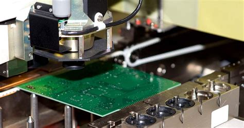
The manufacturing process of HDI PCB 2+4+2, a high-density interconnect printed circuit board, is a sophisticated procedure that requires precision and advanced technology. This type of PCB is characterized by its complex layer structure, which includes two outer layers, four inner layers, and two additional layers, making it ideal for applications demanding high performance and miniaturization. The process begins with the selection of suitable materials, typically high-quality laminates and copper foils, which are essential for ensuring the board’s reliability and performance.
Initially, the inner layers are fabricated through a process known as inner layer imaging.
This involves coating the copper-clad laminate with a photosensitive film, followed by exposure to ultraviolet light through a photomask that defines the circuit pattern. The exposed areas are then developed, revealing the copper that needs to be etched away. The etching process removes the unwanted copper, leaving behind the desired circuit pattern. Subsequently, the inner layers undergo an oxide treatment to enhance the adhesion between layers during the lamination process.
Following the preparation of the inner layers, the next step is lamination.
This involves stacking the inner layers with prepreg sheets, which are layers of fiberglass impregnated with resin, and outer copper foils. The stack is then subjected to heat and pressure in a lamination press, causing the resin to flow and bond the layers together, forming a solid multilayer board. This step is crucial for ensuring the structural integrity and electrical performance of the HDI PCB.
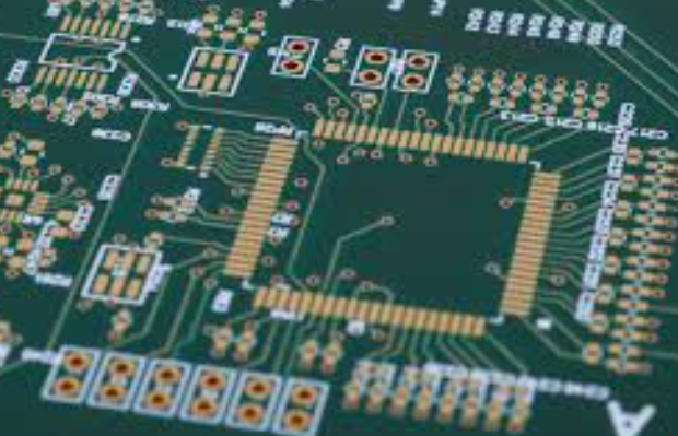
Once the lamination is complete, the board undergoes drilling to create vias, which are small holes that allow electrical connections between different layers.
In HDI PCBs, microvias are commonly used due to their smaller size and ability to increase circuit density. These microvias are typically formed using laser drilling, which offers precision and accuracy. After drilling, the vias are plated with copper through an electroplating process, ensuring reliable electrical connections.
The next phase involves outer layer imaging, similar to the inner layer process, where the outermost copper layers are patterned to form the circuit traces.
This is followed by solder mask application, where a protective layer is applied to prevent solder bridging and protect the circuit from environmental factors. The solder mask is typically applied using a screen-printing process and then cured to form a durable coating.
Subsequently, the board undergoes surface finish application, which is essential for ensuring good solderability and protecting the exposed copper surfaces.
Common finishes include ENIG (Electroless Nickel Immersion Gold), HASL (Hot Air Solder Leveling), and OSP (Organic Solderability Preservative), each offering distinct advantages depending on the application requirements.
Finally, the HDI PCB 2+4+2 is subjected to electrical testing to verify its functionality and ensure there are no defects. This involves checking for continuity and isolation between the various circuit paths. Once the board passes all quality checks, it is ready for assembly and integration into electronic devices. The meticulous nature of the manufacturing process ensures that HDI PCBs meet the high standards required for modern electronic applications, where space constraints and performance demands continue to grow.
Applications Of HDI PCB 2+4+2 In Modern Electronics
High-Density Interconnect (HDI) Printed Circuit Boards (PCBs) have become a cornerstone in the advancement of modern electronics, offering enhanced performance and miniaturization capabilities. Among the various configurations of HDI PCBs, the 2+4+2 structure stands out due to its unique layering and interconnectivity features.
This configuration is particularly significant in applications where space constraints and high performance are critical. The 2+4+2 HDI PCB consists of two outer layers, four inner layers, and two additional layers, which are often used for routing complex circuits. This structure allows for a higher density of components and interconnections, making it ideal for a range of modern electronic applications.
One of the primary applications of HDI PCB 2+4+2 is in the realm of consumer electronics, where devices are continually becoming more compact and multifunctional.
Smartphones, for instance, benefit greatly from the compactness and efficiency of HDI PCBs. The 2+4+2 configuration allows for the integration of more components in a smaller area, which is essential for the slim designs of modern smartphones. This not only enhances the device’s functionality but also improves its performance by reducing the distance that electrical signals must travel, thereby increasing speed and efficiency.
In addition to consumer electronics, the automotive industry has also embraced the use of HDI PCB 2+4+2.
As vehicles become more technologically advanced, with features such as advanced driver-assistance systems (ADAS), infotainment systems, and electric powertrains, the demand for compact and reliable electronic components has surged. The 2+4+2 configuration supports the integration of complex electronic systems within the limited space available in vehicles. This is crucial for maintaining the performance and reliability of automotive electronics, which are subject to harsh operating conditions.
Moreover, the medical field has seen significant advancements with the adoption of HDI PCB 2+4+2.
Medical devices, such as portable diagnostic equipment and implantable devices, require high precision and reliability. The compact nature of the 2+4+2 configuration allows for the development of smaller, more efficient medical devices that can perform complex functions. This is particularly important in applications where device size and weight are critical factors, such as in wearable health monitors and implantable sensors.
Furthermore, the aerospace and defense sectors have also leveraged the benefits of HDI PCB 2+4+2.
In these industries, the need for lightweight, compact, and highly reliable electronic systems is paramount. The 2+4+2 configuration provides the necessary density and performance required for sophisticated avionics and defense systems. These systems often operate in extreme environments, where reliability and performance cannot be compromised. The robust nature of HDI PCBs ensures that these systems can withstand such conditions while maintaining optimal functionality.
In conclusion, the HDI PCB 2+4+2 configuration plays a pivotal role in the advancement of modern electronics across various industries.
Its ability to support high-density component placement and complex interconnections makes it an invaluable asset in the development of compact, efficient, and high-performance electronic devices. As technology continues to evolve, the demand for such advanced PCB configurations is expected to grow, further cementing their importance in the future of electronics.
Challenges In HDI PCB 2+4+2 Fabrication
The fabrication of High-Density Interconnect (HDI) Printed Circuit Boards (PCBs) has become increasingly complex as the demand for more compact and efficient electronic devices continues to rise. Among the various configurations, the 2+4+2 HDI PCB structure presents unique challenges that require careful consideration and advanced manufacturing techniques. This configuration, characterized by two outer layers, four inner layers, and two additional layers, is designed to accommodate higher component density and improved electrical performance. However, the intricacies involved in its fabrication pose significant hurdles that manufacturers must overcome.
One of the primary challenges in fabricating 2+4+2 HDI PCBs is the precise alignment required during the multilayer lamination process.
As the number of layers increases, so does the complexity of ensuring that each layer is perfectly aligned with the others. Misalignment can lead to electrical failures and reduced performance, necessitating the use of advanced alignment technologies and meticulous quality control measures. Moreover, the increased layer count also demands more sophisticated drilling techniques to create the microvias that connect the different layers. These microvias must be drilled with extreme precision to maintain the integrity of the electrical connections, which can be particularly challenging given the reduced space available in HDI designs.
In addition to alignment and drilling challenges, the materials used in 2+4+2 HDI PCBs must be carefully selected to withstand the thermal and mechanical stresses encountered during operation.
The choice of substrate material is critical, as it must provide the necessary thermal stability and electrical insulation while also being compatible with the other materials used in the board. Furthermore, the copper used for the conductive traces must be of high quality to ensure reliable signal transmission and minimize the risk of signal loss or interference. The integration of these materials requires a deep understanding of their properties and how they interact under various conditions.
Another significant challenge is the implementation of advanced manufacturing processes such as laser drilling and sequential lamination.
These processes are essential for achieving the high precision and density required in 2+4+2 HDI PCBs, but they also introduce additional complexities. Laser drilling, for instance, must be carefully controlled to prevent damage to the surrounding materials, while sequential lamination requires precise temperature and pressure control to ensure proper bonding of the layers. These processes demand a high level of expertise and sophisticated equipment, which can increase production costs and lead times.
Furthermore, the testing and inspection of 2+4+2 HDI PCBs present their own set of challenges.
Given the complexity and density of these boards, traditional inspection methods may not be sufficient to detect all potential defects. Advanced testing techniques, such as automated optical inspection (AOI) and X-ray inspection, are often required to ensure the quality and reliability of the final product. These methods allow for the detection of hidden defects that could compromise the performance of the PCB, but they also require significant investment in technology and training.
In conclusion, the fabrication of 2+4+2 HDI PCBs involves a multitude of challenges that stem from their complex structure and the high demands placed on their performance.
From precise alignment and drilling to material selection and advanced manufacturing processes, each step in the fabrication process requires careful consideration and expertise. As technology continues to evolve, manufacturers must remain vigilant in addressing these challenges to produce reliable and efficient HDI PCBs that meet the ever-growing demands of the electronics industry.