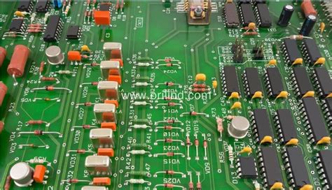
Hdi pcb any layer
Advantages Of HDI PCB Any Layer Technology
High-Density Interconnect (HDI) Printed Circuit Boards (PCBs) have revolutionized the electronics industry by enabling the design and manufacture of more compact, efficient, and powerful electronic devices. Among the various types of HDI PCBs, the “any layer” technology stands out due to its unique advantages, which have made it a preferred choice for many advanced applications. This article explores the benefits of HDI PCB any layer technology, highlighting its impact on modern electronics.
To begin with, HDI PCB any layer technology allows for the interconnection of all layers of a PCB, providing designers with unparalleled flexibility.
This capability is particularly beneficial in the development of complex electronic devices where space is at a premium. By enabling connections between any two layers, this technology facilitates the creation of more intricate and compact designs, which is essential for devices such as smartphones, tablets, and wearable technology. The ability to interconnect any layer also reduces the need for through-hole vias, which can take up valuable space and limit design options.
Moreover, the use of HDI PCB any layer technology significantly enhances the electrical performance of a device.
The reduction in the number of through-hole vias not only saves space but also minimizes signal loss and electromagnetic interference. This is crucial for high-speed applications where signal integrity is paramount. The shorter and more direct routing paths made possible by any layer technology lead to improved signal quality and faster data transmission rates, which are critical for modern communication devices and computing systems.
In addition to improved electrical performance, HDI PCB any layer technology contributes to the overall reliability and durability of electronic devices.
The elimination of through-hole vias reduces the mechanical stress on the board, which can be a source of failure in traditional PCB designs. Furthermore, the use of microvias, which are a hallmark of HDI technology, enhances the thermal performance of the board. This is particularly important in high-power applications where efficient heat dissipation is necessary to prevent overheating and ensure long-term reliability.
Another significant advantage of HDI PCB any layer technology is its contribution to the miniaturization of electronic devices.
As consumer demand for smaller, lighter, and more portable devices continues to grow, manufacturers are under pressure to deliver products that meet these expectations. HDI PCB any layer technology enables the production of smaller PCBs without compromising on functionality or performance. This is achieved by increasing the density of components on the board, allowing for more features to be packed into a smaller footprint.
Furthermore, the adoption of HDI PCB any layer technology can lead to cost savings in the manufacturing process.
While the initial design and setup costs may be higher compared to traditional PCBs, the long-term benefits often outweigh these expenses. The reduction in board size and the number of layers can lead to lower material costs, and the improved reliability can result in fewer returns and warranty claims. Additionally, the enhanced performance and functionality can provide a competitive edge in the market, potentially leading to increased sales and revenue.
In conclusion, HDI PCB any layer technology offers numerous advantages that make it an attractive option for modern electronic device design and manufacturing. Its ability to provide flexible interconnections, improve electrical performance, enhance reliability, enable miniaturization, and reduce costs underscores its significance in the ever-evolving electronics industry. As technology continues to advance, the role of HDI PCB any layer technology is likely to become even more prominent, driving innovation and shaping the future of electronic devices.
Design Considerations For HDI PCB Any Layer
When designing High-Density Interconnect (HDI) Printed Circuit Boards (PCBs) with any layer interconnects, several critical considerations must be taken into account to ensure optimal performance and reliability. HDI technology, characterized by its ability to accommodate more components in a smaller area, is increasingly favored in applications requiring miniaturization and enhanced functionality. The any layer approach, which allows interconnections between any two layers of the PCB, further enhances design flexibility and circuit density. However, this complexity necessitates a thorough understanding of various design elements.
To begin with, the choice of materials is paramount.
HDI PCBs often employ advanced materials that can withstand higher temperatures and offer better electrical performance. These materials must be carefully selected to match the specific requirements of the application, considering factors such as dielectric constant, thermal expansion, and mechanical strength. The use of high-quality materials not only ensures the durability of the PCB but also contributes to its overall performance.
Moreover, the design of via structures is a crucial aspect of HDI PCB design.
In any layer HDI, microvias are typically used to connect different layers. These microvias, which are much smaller than traditional vias, allow for greater routing density and improved electrical performance. However, their implementation requires precision to avoid issues such as misalignment or incomplete drilling, which can lead to circuit failures. Therefore, employing advanced drilling techniques and thorough inspection processes is essential to maintain the integrity of these connections.
Another important consideration is the layer stack-up configuration.
The stack-up must be meticulously planned to optimize signal integrity and minimize electromagnetic interference (EMI). This involves determining the appropriate number of layers and their arrangement to ensure efficient power distribution and signal routing. Additionally, the use of ground and power planes can help in reducing EMI and improving signal quality. Designers must also consider the impedance control, which is critical for high-speed applications, to prevent signal degradation.
Thermal management is another key factor in HDI PCB design.
As the density of components increases, so does the potential for heat generation. Effective thermal management strategies, such as the use of thermal vias, heat sinks, and appropriate material selection, are necessary to dissipate heat and maintain the reliability of the PCB. Failure to address thermal issues can lead to overheating, which may compromise the performance and lifespan of the board.
Furthermore, the manufacturability of the HDI PCB must be considered during the design phase.
The complexity of any layer HDI designs can pose challenges in fabrication, requiring advanced manufacturing techniques and equipment. Collaborating closely with manufacturers during the design process can help identify potential issues early and ensure that the design is feasible and cost-effective to produce.
In conclusion, designing HDI PCBs with any layer interconnects involves a comprehensive approach that addresses material selection, via structure design, layer stack-up configuration, thermal management, and manufacturability. By carefully considering these factors, designers can create PCBs that meet the demanding requirements of modern electronic applications, providing enhanced performance and reliability. As technology continues to evolve, the importance of meticulous design in HDI PCBs will only grow, underscoring the need for expertise and precision in this field.
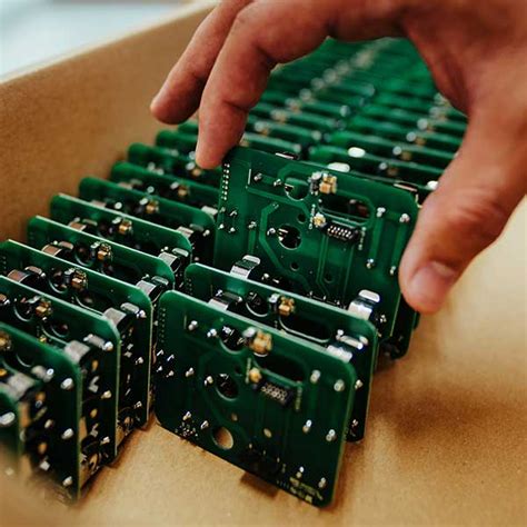
Manufacturing Process Of HDI PCB Any Layer
The manufacturing process of HDI (High-Density Interconnect) PCBs, particularly those with any-layer technology, represents a significant advancement in the field of printed circuit board design and production. This sophisticated process is essential for creating compact, high-performance electronic devices that are increasingly in demand in today’s technology-driven world. To understand the intricacies of this process, it is crucial to explore the various stages involved, each of which contributes to the overall functionality and reliability of the final product.
Initially, the process begins with the selection of appropriate materials.
The choice of substrate is critical, as it must support the high-density interconnections and withstand the thermal and mechanical stresses encountered during operation. Typically, materials such as FR-4, a glass-reinforced epoxy laminate, are used due to their excellent electrical insulation properties and mechanical strength. However, for more advanced applications, materials with superior thermal and electrical characteristics may be selected.
Following material selection, the design phase is undertaken, where the layout of the PCB is meticulously planned using advanced computer-aided design (CAD) software.
This stage involves defining the placement of components, the routing of traces, and the configuration of vias, which are essential for connecting different layers of the PCB. In any-layer HDI PCBs, microvias are employed extensively, allowing for interconnections between any two layers without the need for through-hole vias. This capability significantly enhances the design flexibility and density of the PCB.
Once the design is finalized, the manufacturing process proceeds with the fabrication of the individual layers.
This involves the application of a photoresist to the substrate, followed by exposure to ultraviolet light through a photomask that defines the circuit pattern. The exposed areas are then developed, revealing the underlying copper, which is subsequently etched away to form the desired circuit traces. This process is repeated for each layer, with precise alignment being crucial to ensure the integrity of the interconnections.
The next stage involves the drilling of microvias, which is a defining feature of any-layer HDI PCBs.
Laser drilling is typically employed due to its precision and ability to create extremely small vias with high aspect ratios. These microvias are then plated with copper to establish electrical connections between the layers. The use of microvias not only allows for greater design flexibility but also reduces the overall size and weight of the PCB, making it ideal for compact electronic devices.
Subsequently, the individual layers are laminated together under heat and pressure to form a single, cohesive unit.
This lamination process is critical, as it ensures the mechanical stability and electrical integrity of the PCB. Following lamination, additional processes such as surface finishing, solder mask application, and silkscreen printing are performed to prepare the PCB for component assembly.
Finally, rigorous testing and inspection are conducted to verify the functionality and reliability of the HDI PCB. This includes electrical testing to ensure continuity and isolation, as well as visual inspection to detect any defects or anomalies. The culmination of these meticulous processes results in a high-performance HDI PCB with any-layer capability, ready to meet the demands of modern electronic applications. Through this comprehensive manufacturing process, HDI PCBs continue to push the boundaries of what is possible in electronic design and innovation.
Applications Of HDI PCB Any Layer In Modern Electronics
High-Density Interconnect (HDI) Printed Circuit Boards (PCBs) have become a cornerstone in the advancement of modern electronics, particularly with the advent of the “any layer” design. This innovative approach allows for interconnections between all layers of the PCB, offering unprecedented flexibility and efficiency in electronic design. The applications of HDI PCB any layer technology are vast and varied, reflecting its critical role in the evolution of electronic devices.
To begin with, the telecommunications industry has greatly benefited from HDI PCB any layer technology.
As the demand for faster and more reliable communication networks grows, the need for compact and efficient circuit designs becomes paramount. HDI PCBs, with their ability to support higher wiring density and finer lines, enable the development of smaller, more powerful devices. This is particularly evident in smartphones, where space is at a premium, and every millimeter counts. The any layer design allows for more components to be packed into a smaller area, enhancing the device’s functionality without increasing its size.
Moreover, the consumer electronics sector has also seen significant advancements due to HDI PCB any layer technology.
Devices such as tablets, laptops, and wearable technology require lightweight and compact designs without compromising performance. The any layer approach facilitates the integration of multiple functionalities into a single device, thereby improving user experience. For instance, in wearable technology, where flexibility and size are crucial, HDI PCBs provide the necessary support for complex circuitry in a compact form factor.
In addition to consumer electronics, the automotive industry is another area where HDI PCB any layer technology is making a substantial impact.
Modern vehicles are increasingly reliant on electronic systems for everything from engine control to infotainment systems. The any layer design allows for the integration of these diverse systems into a cohesive unit, improving reliability and performance. Furthermore, as the industry moves towards electric and autonomous vehicles, the need for advanced electronic systems becomes even more pronounced. HDI PCBs offer the necessary infrastructure to support these innovations, ensuring that vehicles are both efficient and safe.
Furthermore, the medical field has also embraced HDI PCB any layer technology, particularly in the development of medical devices.
The precision and reliability offered by HDI PCBs are crucial in applications where accuracy is paramount. Devices such as pacemakers, hearing aids, and diagnostic equipment benefit from the compact and efficient design enabled by any layer technology. This not only improves the functionality of these devices but also enhances patient comfort and outcomes.
In the realm of aerospace and defense, HDI PCB any layer technology is indispensable.
The stringent requirements for reliability and performance in these sectors necessitate the use of advanced circuit board designs. HDI PCBs provide the necessary support for complex systems, ensuring that they can withstand the harsh conditions often encountered in these applications. The ability to integrate multiple layers and functionalities into a single board is particularly beneficial in reducing weight and space, which are critical considerations in aerospace design.
In conclusion, the applications of HDI PCB any layer technology in modern electronics are extensive and diverse. From telecommunications and consumer electronics to automotive, medical, and aerospace industries, this technology is driving innovation and efficiency. As electronic devices continue to evolve, the role of HDI PCB any layer technology will undoubtedly become even more significant, paving the way for the next generation of electronic advancements.