Hdi pcb capability
Understanding HDI PCB Capability: Key Features and Benefits
High-Density Interconnect (HDI) Printed Circuit Boards (PCBs) represent a significant advancement in the field of electronics manufacturing, offering a range of capabilities that cater to the ever-evolving demands of modern technology. As electronic devices become increasingly compact and complex, the need for efficient and reliable circuit board solutions has never been more critical. HDI PCBs address these needs by providing enhanced performance, improved functionality, and greater design flexibility, making them an indispensable component in the development of cutting-edge electronic products.
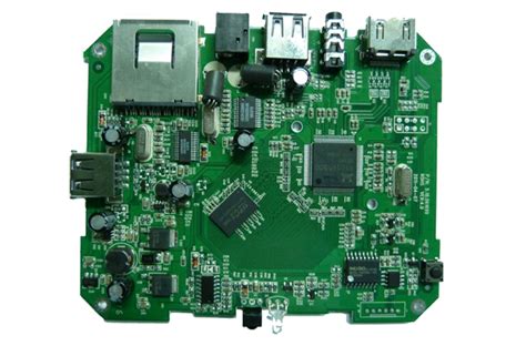
One of the key features of HDI PCBs is their ability to accommodate a higher density of components on a smaller board area.
This is achieved through the use of finer lines and spaces, smaller vias, and capture pads, as well as higher connection pad density. By incorporating these elements, HDI PCBs can support more complex circuitry without increasing the overall size of the board. This capability is particularly beneficial in the design of compact devices such as smartphones, tablets, and wearable technology, where space is at a premium.
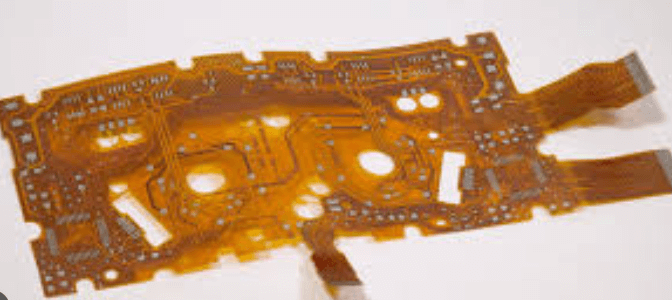
Moreover, HDI PCBs are characterized by their use of microvias, which are significantly smaller than traditional vias.
Microvias allow for more efficient routing of electrical signals between layers, reducing the need for long trace paths and thereby minimizing signal loss and interference. This results in improved electrical performance, which is crucial for high-speed applications and devices that require rapid data processing. Additionally, the use of microvias contributes to the overall reliability of the PCB by reducing the risk of defects and failures associated with larger, more complex via structures.
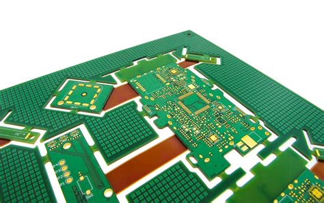
Another notable advantage of HDI PCBs is their ability to support advanced design techniques such as blind and buried vias, as well as sequential lamination.
These techniques enable designers to create multi-layer boards with intricate interconnections, further enhancing the board’s functionality and performance. The ability to incorporate multiple layers also allows for greater design flexibility, enabling engineers to optimize the layout for specific applications and requirements. This is particularly advantageous in industries such as aerospace, automotive, and medical devices, where precision and reliability are paramount.
In addition to their technical capabilities, HDI PCBs offer several practical benefits that contribute to their widespread adoption.
For instance, the reduced size and weight of HDI PCBs make them ideal for portable and lightweight devices, which are increasingly in demand in today’s market. Furthermore, the enhanced performance and reliability of HDI PCBs can lead to longer product lifespans and reduced maintenance costs, providing a cost-effective solution for manufacturers and end-users alike.
As technology continues to advance, the demand for HDI PCBs is expected to grow, driven by the need for more sophisticated and compact electronic devices. Manufacturers are continually refining their processes and materials to further enhance the capabilities of HDI PCBs, ensuring that they remain at the forefront of innovation in the electronics industry. In conclusion, the key features and benefits of HDI PCB capability make it an essential component in the development of modern electronic products, offering a combination of performance, reliability, and design flexibility that is unmatched by traditional PCB technologies.
Design Considerations for HDI PCB Capability in Modern Electronics
In the rapidly evolving landscape of modern electronics, the demand for more compact, efficient, and high-performance devices has led to significant advancements in printed circuit board (PCB) technology. Among these advancements, High-Density Interconnect (HDI) PCBs have emerged as a pivotal innovation, offering enhanced capabilities that cater to the intricate requirements of contemporary electronic designs. As designers and engineers strive to push the boundaries of what is possible, understanding the design considerations for HDI PCB capability becomes crucial.
HDI PCBs are characterized by their ability to accommodate a higher density of components and interconnections within a smaller footprint.
This is achieved through the use of finer lines and spaces, smaller vias, and more layers compared to traditional PCBs. Consequently, HDI technology enables the integration of more functionality into a single board, which is particularly beneficial for applications where space is at a premium, such as in smartphones, tablets, and wearable devices. However, the transition to HDI PCBs necessitates a comprehensive understanding of several design considerations to fully leverage their potential.
One of the primary considerations in HDI PCB design is the selection of materials.
The materials used must support the finer features and higher layer counts typical of HDI designs. This often involves choosing substrates with superior thermal and mechanical properties to ensure reliability and performance. Additionally, the choice of materials can impact the manufacturability and cost of the PCB, making it essential to strike a balance between performance requirements and budget constraints.
Another critical aspect is the design of the via structures.
HDI PCBs commonly employ microvias, which are significantly smaller than traditional vias and can be placed directly on top of each other in a stacked configuration. This allows for more efficient use of space and improved signal integrity. However, the design and fabrication of microvias require precise control and advanced manufacturing techniques to avoid issues such as via failure or signal degradation. Therefore, careful consideration must be given to the via aspect ratio, plating processes, and thermal management to ensure robust performance.
Signal integrity is another vital consideration in HDI PCB design.
As the density of interconnections increases, so does the potential for signal interference and loss. To mitigate these challenges, designers must employ advanced simulation tools and techniques to optimize trace routing, impedance control, and layer stack-up. This often involves iterative design processes and close collaboration with manufacturers to ensure that the final product meets the desired electrical performance specifications.
Thermal management also plays a crucial role in the design of HDI PCBs.
The compact nature of these boards can lead to increased heat generation, which, if not properly managed, can adversely affect the performance and longevity of the device. Effective thermal management strategies, such as the use of thermal vias, heat sinks, and appropriate material selection, are essential to dissipate heat efficiently and maintain optimal operating conditions.
In conclusion, the design considerations for HDI PCB capability in modern electronics are multifaceted and require a holistic approach. By carefully addressing material selection, via design, signal integrity, and thermal management, designers can harness the full potential of HDI technology to create innovative and high-performance electronic devices. As the demand for miniaturization and functionality continues to grow, HDI PCBs will undoubtedly play an increasingly important role in shaping the future of electronics.
Advancements in HDI PCB Capability: Trends and Innovations
High-Density Interconnect (HDI) printed circuit boards (PCBs) have become a cornerstone in the evolution of modern electronics, driven by the relentless demand for more compact, efficient, and powerful devices. As technology continues to advance, the capabilities of HDI PCBs have expanded significantly, enabling the development of increasingly sophisticated electronic products. This article explores the latest trends and innovations in HDI PCB capability, highlighting the technological advancements that are shaping the future of electronics manufacturing.
To begin with, one of the most notable trends in HDI PCB technology is the miniaturization of electronic components.
As consumer electronics, such as smartphones and wearable devices, become smaller and more feature-rich, the need for compact and efficient circuit boards has intensified. HDI PCBs address this demand by utilizing finer lines and spaces, smaller vias, and higher connection pad density. These features allow for more components to be packed into a smaller area, thereby enhancing the functionality of the device without increasing its size. Consequently, manufacturers are increasingly adopting HDI technology to meet the growing consumer expectations for sleek and powerful gadgets.
In addition to miniaturization, the integration of advanced materials is another significant innovation in HDI PCB capability.
Traditional PCBs are typically made from materials like FR-4, which, while effective, have limitations in terms of thermal management and signal integrity. To overcome these challenges, manufacturers are exploring the use of advanced materials such as liquid crystal polymer (LCP) and polytetrafluoroethylene (PTFE). These materials offer superior electrical performance, reduced signal loss, and improved thermal properties, making them ideal for high-frequency applications. As a result, HDI PCBs are becoming increasingly prevalent in industries such as telecommunications, aerospace, and automotive, where performance and reliability are paramount.
Moreover, the advent of laser drilling technology has revolutionized the manufacturing process of HDI PCBs.
Laser drilling allows for the creation of microvias, which are essential for achieving the high-density interconnections that characterize HDI boards. This technology enables the precise drilling of extremely small holes, facilitating the connection of multiple layers within the PCB. The ability to produce microvias with high accuracy and consistency has significantly enhanced the design flexibility and performance of HDI PCBs, allowing for more complex and efficient circuit layouts.
Furthermore, the rise of automation and advanced manufacturing techniques has played a crucial role in advancing HDI PCB capability.
Automated processes, such as robotic assembly and machine learning-driven quality control, have improved the precision and efficiency of PCB production. These technologies not only reduce the likelihood of human error but also enable faster production times and lower costs. As a result, manufacturers can produce high-quality HDI PCBs at scale, meeting the increasing demand for advanced electronic devices.
In conclusion, the advancements in HDI PCB capability are a testament to the rapid pace of innovation in the electronics industry. Through miniaturization, the integration of advanced materials, laser drilling technology, and automation, HDI PCBs have become more capable and versatile than ever before. As these trends continue to evolve, they will undoubtedly pave the way for the next generation of electronic devices, offering enhanced performance, reliability, and functionality. The ongoing development of HDI technology promises to unlock new possibilities in electronics design and manufacturing, driving progress across a wide range of industries.
Challenges and Solutions in HDI PCB Capability Manufacturing
High-Density Interconnect (HDI) printed circuit boards (PCBs) have become a cornerstone in the advancement of modern electronics, offering enhanced performance and miniaturization. However, the manufacturing of HDI PCBs presents a unique set of challenges that require innovative solutions to ensure efficiency and reliability. As the demand for smaller, faster, and more efficient electronic devices continues to grow, manufacturers are compelled to address these challenges with precision and expertise.
One of the primary challenges in HDI PCB manufacturing is the complexity of the design.
HDI PCBs are characterized by their high wiring density per unit area, which necessitates the use of finer lines and spaces, smaller vias, and capture pads. This complexity requires advanced design software and meticulous planning to ensure that the intricate patterns are accurately translated onto the board. Moreover, the need for multiple layers in HDI PCBs further complicates the design process, as it requires precise alignment and registration to maintain the integrity of the connections.
In addition to design complexities, material selection poses another significant challenge.
The materials used in HDI PCBs must possess excellent thermal and electrical properties to withstand the demands of high-speed and high-frequency applications. Manufacturers must carefully select substrates and laminates that offer low dielectric constants and loss tangents, while also being compatible with the fine-pitch components used in HDI designs. Furthermore, the materials must be robust enough to endure the mechanical stresses encountered during the manufacturing process, such as drilling and lamination.
The manufacturing process itself presents several hurdles, particularly in the drilling and plating stages.
The use of microvias, which are essential for HDI PCBs, requires advanced laser drilling techniques to achieve the necessary precision and accuracy. Traditional mechanical drilling methods are often inadequate for the small diameters and high aspect ratios required in HDI designs. Additionally, the plating process must ensure uniform copper deposition within these microvias to maintain electrical connectivity and reliability. This necessitates the use of specialized plating techniques and equipment to achieve consistent results.
To address these challenges, manufacturers have adopted a range of solutions that leverage technological advancements and process innovations.
For instance, the use of laser direct imaging (LDI) technology has significantly improved the accuracy and resolution of the patterning process, enabling the production of finer lines and spaces. Similarly, advancements in material science have led to the development of high-performance substrates that meet the stringent requirements of HDI applications.
Moreover, the implementation of automated manufacturing processes has enhanced the precision and efficiency of HDI PCB production.
Automation reduces the likelihood of human error and ensures consistent quality across large production volumes. Additionally, manufacturers are increasingly utilizing advanced inspection and testing methods, such as automated optical inspection (AOI) and X-ray inspection, to detect and rectify defects early in the production process.
In conclusion, while the manufacturing of HDI PCBs presents a myriad of challenges, the industry has made significant strides in developing solutions that address these complexities. Through the integration of cutting-edge technologies and innovative processes, manufacturers are able to produce HDI PCBs that meet the ever-evolving demands of modern electronics. As technology continues to advance, it is likely that further innovations will emerge, paving the way for even more sophisticated and capable HDI PCB designs.