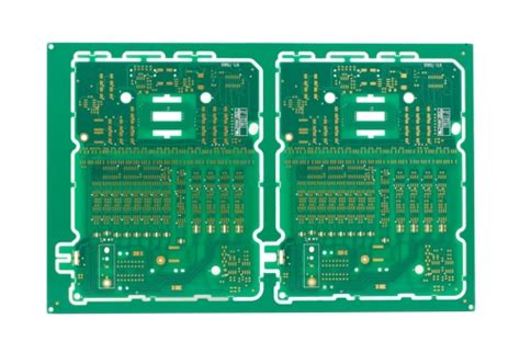
Variations in substrate size during PCB manufacturing
The reason:
(1) The dimensional change of the substrate caused by the difference in the longitude and latitude direction; due to shearing, the fiber orientation is not paid attention to, and the shear stress remains in the substrate. Once released, the size of the substrate is directly affected.
(2) The copper foil portion of the substrate surface is etched away to limit the variation of the substrate, and a dimensional change occurs when the stress is removed.
(3) When the brush plate is used due to excessive pressure, resulting in tensile stress caused by deformation of the substrate.
(4) The resin in the substrate is not completely cured, resulting in a dimensional change.
(5) In particular, prior to lamination of the multilayer board, poor storage conditions cause the thin substrate or prepreg to absorb moisture, resulting in poor dimensional stability.
(6) When laminates are pressed together, excessive flow of glue causes deformation of the glass cloth.
Solutions:
(1) Determine the variation of the latitude and longitude direction.
Compensate on the negative film according to the shrinkage rate (this work is done before light drawing). At the same time, cutting is performed in the direction of the fiber, or in accordance with the character mark provided by the manufacturer on the substrate (usually the longitudinal direction of the character is the longitudinal direction of the substrate).
(2) When designing circuits, the entire board surface should be distributed as evenly as possible.
If it is impossible, it must also leave a transition section in space (does not affect the circuit location mainly). This is due to the differences in the warp and weft strengths of the sheet due to the differences in the warp and weft densities of the sheets in the glass cloth structure.
(3) Test brushes should be used so that the process parameters are in the best condition and then the rigid plates are to be used.
For thin substrates, chemical cleaning or electrolytic processes should be used for cleaning.
(4) Take a baking solution. In particular, the baking is performed before drilling, and the temperature is 120° C.
for 4 hours to ensure that the resin is cured and the deformation of the substrate is reduced due to the effects of cold and heat.
(5) The inner oxidized substrate must be baked to remove moisture.
Store the processed substrate in a vacuum oven to avoid reabsorption.
(6) It is necessary to carry out the process pressure test, adjust the process parameters and then press. At the same time, according to the characteristics of the prepreg, choose the right amount of glue.
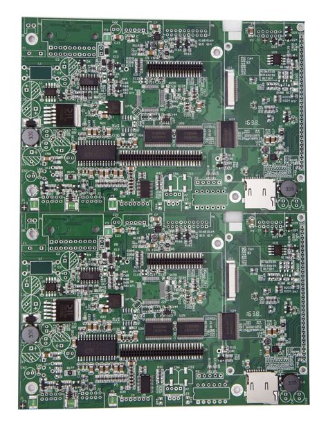
When PCB design, how to control the relationship between line width and current?
For some electromechanical control systems, sometimes the instantaneous current flowing in the trace can reach more than 100A. In this case, the relatively thin line will definitely cause problems.
A basic empirical value is: 10 A/square mm, that is, a current with a cross-sectional area of 1 mm 2 can safely pass 10 A. If the line width is too thin, the trace will burn when high current passes.
Of course, current burned traces must follow the energy formula: Q=I*I*t. For example, for a 10A current trace, a 100A current glitch suddenly occurs for a duration of us, and the 30mil wire is Certainly can withstand.
(There will be another problem at this time: stray inductance of the wire, this glitch will produce a strong back electromotive force under the action of this inductor, which may damage other devices. The thinner the longer the wire spurious. The greater the inductance, so in practice we have to consider the length of the conductor.)
The general PCB drawing software often has several options for copper via pads on the device pins: right angle spokes, 45 degree spokes, and straight shop.
What’s the difference between them? Newcomers don’t care much about it, just pick one and they look beautiful. actually not. There are two main considerations: First, consider that you cannot dissipate heat too quickly, and second, consider overcurrent capability.
The characteristic of using the straight-laid method is that the over-current capability of the pad is very strong, and this method must be used for the device pins on the high-power loop.
At the same time, its thermal conductivity is also very strong, although it works to heat the device, but this is a problem for the board soldering staff, because the pad heat is too fast to hang tin, often need to use a larger wattage soldering iron and Higher welding temperatures reduce production efficiency.
The use of right-angled spokes and 45-degree spokes will reduce the contact area between the pins and the copper foil, slow heat dissipation, and welding will be much easier.
Therefore, the choice of the connection mode of the via pad copper plating should be based on the application, integrated over-current capacity and heat dissipation capabilities together, the small power signal line should not use direct shop, but for the pad through the large current must be straight shop. As for the right angle or 45 degree angle to see beautiful.
Why did you mention this? Because the past has been studying a motor drive, the H bridge device of this drive is always burned, and no reason can be found for four or five years. After some hard work, I finally discovered that it was originally the copper pad of a device in the power circuit that used right-angled spokes when laying copper (and because of poor copper painting, only two spokes actually appeared. ).
This greatly reduces the overcurrent capability of the entire power loop.
Although the product did not have any problems during normal use, it worked perfectly at 10A. However, when a short circuit occurs in the H-bridge, a current of about 100 A appears on the loop, and the two spokes are instantaneously blown (uS level). Then, the power circuit becomes an open circuit, and the energy stored in the motor is emitted through all possible channels without a drain channel.
This energy will burn the current-carrying resistance and related operational amplifier components and destroy the bridge control chip. It also broke into the signal and power supply of the digital circuit, causing serious damage to the entire device.
The whole process is like using a hair wire to detonate a large land mine as thrilling.
Then you may want to ask, why do you only use two spokes on the pad in the power circuit? Why don’t you let copper foil go straight? Because, uh, the production department’s staff said that if this pin is too hard Were welding! The designer just listened to the production staff, so only… Hey, I found this problem really cost me brains, which is as simple as saying! …
If the via hole is less than 0.3mm, there is no way to use mechanical drilling. To use laser drilling, the production and processing of the board is more difficult. So my personal thought is that if not very much needed, the minimum is 0.5mm outside/0.3mm inside. . But like computer motherboards, memory sticks, dense BGA packages, etc., it may be as small as 14mil/8mil.