UV laser application in various PCB materials
Ultraviolet lasers are the best choice for a variety of PCB materials in many industrial applications, from the most basic circuit boards, circuit wiring, to advanced processes such as pocket-sized embedded chips. The variability of this material makes UV lasers the best choice for a wide range of PCB materials in many industrial applications, from the most basic boards, circuit wiring, to advanced processes such as pocket-sized embedded chips.
Application 1: Surface Etching / Circuit Production
Ultraviolet lasers work quickly in the production of circuits, and surface patterns can be etched onto the board in minutes. This makes UV lasers the fastest way to produce PCB samples. The R&D department noted that more and more sample laboratories are being equipped with internal UV laser systems.
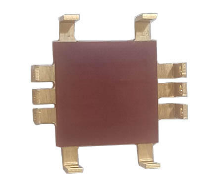
Depending on the optical instrument verification, the UV laser beam can be 10-20 μm in size, producing flexible circuit traces. The application in Figure 2 shows the greatest advantage of UV in the production of circuit traces, which are extremely small and need to be visible under a microscope.
The board measures 0.75″ x 0.5″ and consists of a sintered ceramic substrate and a tungsten/nickel/copper/surface. The laser is capable of producing 2 mils of circuit traces at a distance of 1 mil, resulting in a total pitch of only 3 mils.
Although the use of laser beam production circuits is the fastest method of PCB samples, large-scale surface etching applications are best left to the chemical process.
Application 2: PCB removal
Ultraviolet laser cutting is an excellent choice for large or small production, and it is also a good choice for PCB disassembly, especially when it is needed on flexible or rigid-flex boards. Disassembly is the removal of a single board from the panel. Considering the increasing flexibility of the material, this disassembly poses a major challenge.
Mechanical disassembly methods such as V-groove cutting and automatic board cutting tend to damage sensitive and slim substrates, causing trouble for electronic professional manufacturing service (EMS) companies to disassemble flexible and rigid-flex circuit boards.
Ultraviolet laser cutting not only eliminates the effects of mechanical stresses during detachment processes such as edging, deformation, and damage to circuit components, but also has less thermal stress effects than other lasers such as CO2 laser cutting.
The reduction in “cutting cushions” saves space, which means that components can be placed closer to the edge of the line, and more lines can be installed on each board to maximize efficiency for maximum flexibility in flexible line applications. .
Application 3: Drilling
Another application that utilizes the small beam size and low stress properties of UV lasers is drilling, including through holes, microvias, and blind vias. The UV laser system drills through a focused vertical beam that cuts through the substrate. Depending on the material used, holes as small as 10 μm can be drilled.
Ultraviolet lasers are especially useful for multi-layer drilling. Multilayer PCBs are thermoformed together using composite materials. These so-called “semi-cured” separations occur, especially after processing with higher temperature lasers. However, the relatively stress-free properties of UV lasers solve this problem, as shown in Figure 4.
A 4 mil diameter hole was drilled into a 14 mil multi-layer panel on the cross-section shown. This application on a flexible polyimide copper plated substrate shows no separation between the layers. With regard to the low stress properties of UV lasers, it is also important to improve the yield data. Yield is the percentage of available boards that are removed from a panel.
In the manufacturing process, many conditions can cause damage to the board, including broken solder joints, broken components or delamination. Either factor can cause the board to be thrown into the waste bin on the production line rather than entering the shipping box.
Application 4: Deep engraving
Another application that demonstrates the versatility of UV lasers is deep engraving, which takes many forms. Using software control of the laser system, the laser beam is set to perform controlled ablation, ie to be able to cut on a material at the required depth, to stop, continue and complete before switching to another depth and starting another task Processing.
Various depth applications include small-scale production for embedding chips and surface grinding to remove organic materials from metal surfaces.
Ultraviolet lasers can also perform multi-step operations on the substrate. On polyethylene, the first step is to use a laser to create a groove with a depth of 2 mils, the second step is to create an 8 mils groove on the basis of the previous step, and the third step is a 10 mil groove. This illustrates the overall user control functionality provided by the UV laser system.
Conclusion: A versatile approach
The most striking thing about UV lasers is the ability to do all of these applications in a single step. What does this mean for manufacturing a circuit board? There is no longer a need to use an influential process and method to accomplish an application on different equipment, and a complete part can be obtained in a single process.
This streamlined production solution helps eliminate quality control issues that arise when boards are switched between processes. Ultraviolet-free debris-free ablation also means no post-processing cleaning is required.
PCB board impedance board definition
First, the printed circuit board impedance characteristics:
According to the theory of signal transmission, the signal is a function of time and distance variables, so each part of the signal may change on the line. Therefore, the AC impedance of the connection, that is, the ratio of the change of the voltage to the change of the current is determined as the characteristic impedance of the transmission line:
the characteristic impedance of the transmission line is only related to the characteristics of the signal connection itself. In the actual circuit, the resistance value of the wire itself is smaller than the distributed impedance of the system. In the high-frequency circuit, the characteristic impedance mainly depends on the distributed capacitance of the unit distributed capacitance and the unit distributed inductance. The characteristic impedance of an ideal transmission line depends only on the unit distribution capacitance of the connection and the unit distribution inductance.
Second, the calculation of the characteristic impedance of the printed circuit board:
The proportional relationship between the rising edge time of the signal and the time required for the signal to be transmitted to the receiving end determines whether the signal connection is considered to be the transmission line. The specific proportional relationship can be explained by the following formula: If the length of the wire connection on the PCB is greater than l/b, the connecting wire between the signals can be regarded as the transmission line.
According to the calculation formula of the equivalent impedance of the signal, the impedance of the transmission line can be expressed by the following formula: wL>>R is satisfied in the case of high frequency (tens of megahertz to several hundred megahertz) (of course, in the range where the signal frequency is greater than 109 Hz, Considering the skin effect of the signal, this relationship needs to be carefully studied). Then for a certain transmission line, its characteristic impedance is a constant. The reflection phenomenon of the signal is caused by the inconsistency between the characteristic impedance of the driving end of the signal and the transmission line and the impedance of the receiving end. For a CMOS circuit, the output impedance of the driver end of the signal is relatively small, tens of ohms. The input impedance of the receiving end is relatively large.
Third, printed circuit board characteristic impedance control:
The characteristic impedance of the conductor on the printed circuit board is an important indicator of the circuit design. Especially in the PCB design of the high frequency circuit, it must be considered whether the characteristic impedance of the wire and the characteristic impedance required by the device or signal are consistent and matched. Therefore, there are two concepts that must be noted in the reliability design of PCB design.
Fourth, printed circuit board impedance control:
There are various signal transmissions in the conductors in the circuit board. When the transmission frequency must be increased, the frequency must be increased. If the circuit itself is different due to etching, laminate thickness, wire width, etc., the impedance value will be changed. Signal distortion. Therefore, the conductor on the high-speed circuit board, the impedance value should be controlled within a certain range, called “impedance control.”
The factors affecting the impedance of the PCB trace are mainly the width of the copper wire, the thickness of the copper wire, the dielectric constant of the medium, the thickness of the medium, the thickness of the pad, the path of the ground line, and the trace around the trace. Therefore, when designing the PCB, the impedance of the board trace must be controlled to avoid signal reflection and other electromagnetic interference and signal integrity problems as much as possible to ensure the stability of the actual use of the PCB board. The calculation method of the microstrip line and stripline impedance on the PCB can refer to the corresponding empirical formula.
Fifth, the printed circuit board impedance matching:
In the circuit board, if there is a signal transmission, it is desirable to be smoothly transmitted to the receiving end from the emitting end of the power source with minimal energy loss, and the receiving end completely absorbs it without any reflection. To achieve this type of transmission, the impedance in the line must be equal to the impedance inside the emitting end to be called “impedance matching.”
Impedance matching is one of the design elements when designing high speed PCB circuits. The impedance value has an absolute relationship with the routing method. For example, whether the distance between the surface layer (Microstrip) or the inner layer (Stripline/Double Stripline), the reference power layer or the ground layer, the trace width, and the PCB material affect the characteristic impedance of the trace.
That is to say, the impedance value can be determined after wiring, and the characteristic impedance produced by different PCB manufacturers is also slightly different. General simulation software can not consider some discontinuous wiring conditions due to the limitation of the circuit model or the mathematical algorithm used. At this time, only some terminators (Temninators), such as series resistors, can be reserved on the schematic. Moderate the effect of discontinuity in the trace impedance. The only way to solve the problem is to pay attention to avoiding impedance discontinuities.