LED aluminum substrate process and material selection
The aluminum substrate PCB consists of a circuit layer (copper foil layer), a thermally conductive insulating layer, and a metal base layer. The circuit layer requires a large current-carrying capacity, so thick copper foil should be used, and the thickness is generally 35μm~280μm.
The thermal insulation layer is the core technology of the PCB aluminum substrate, and it is generally a special polymer filled with special ceramics.
Composition, small thermal resistance, excellent viscoelastic properties, ability to resist heat aging, able to withstand mechanical and thermal stress.
The thermal insulation layers of high-performance PCB aluminum substrates such as IMS-H01, IMS-H02 and LED-0601 are using this technology, making them extremely excellent in thermal conductivity and high-strength electrical insulation; the metal substrate is an aluminum substrate. The support members are required to have high thermal conductivity, generally aluminum plates, and copper plates (where copper plates can provide better thermal conductivity), and are suitable for conventional mechanical processing such as drilling, punching and cutting. Process requirements are: gold plating, spray tin, osp anti-oxidation, gold sink, lead-free ROHS process and so on.
Detailed product description:
Substrate, aluminum substrate Product features: thin insulation layer, small thermal resistance; non-magnetic; good heat dissipation; high mechanical strength; product standard thickness: 0.8, 1.0, 1.2, 1.5, 2.0, 2.5, 3.0mm Copper foil thickness: 1.8um 35um 70um 105um 140um Features: High heat dissipation, electromagnetic shielding, high mechanical strength, excellent processing performance. Uses: LED dedicated power hybrid IC (HIC).
The aluminum substrate is to carry the heat conduction of the LED and the device, and the heat dissipation mainly depends on the area.
Concentrated heat conduction can select a plate with a high thermal conductivity coefficient, such as the United States begs plate; slow heat conduction or heat dissipation domestic general materials can be. The price difference is relatively large, the production of finished products begs plate will need more than 4,000 yuan square meters, the general domestic material is more than 1000 yuan square meters. The general use voltage of LED is not very high, choose 1mil thickness insulating layer pressure is greater than 2000V can.
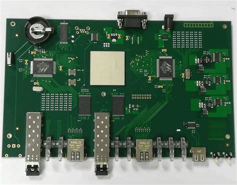
Detailed PCB layout technology
First: Early preparations. This includes preparing component libraries and schematics. “If a worker wants to do something good, he must first sharpen his tools.” To make a good board, in addition to designing principles, he must paint well. Before doing PCB design, we must first prepare the schematic SCH’s component library and PCB’s component library.
Component library can use peotel’s own library, but in general it is difficult to find a suitable, it is best to do their own component library based on the standard size of the selected device. In principle, first do the PCB’s component library, and then do SCH’s component library. The requirements of the PCB’s component library are relatively high. It directly affects the installation of the board.
The SCH’s component library requirements are relatively loose, as long as you pay attention to defining the pin attributes and the corresponding relationship with the PCB components. PS: Note the hidden pins in the standard library. After that is the schematic design, ready to start doing PCB design.
Second: PCB structure design. In this step, according to the determined circuit board size and various mechanical positioning, the PCB board surface is drawn in the PCB design environment, and the required connectors, buttons/switches, screw holes, assembly holes, etc. are placed according to the positioning requirements. And fully consider and determine the wiring area and non-wiring area (for example, the extent of screw holes around the non-routing area).
Third: PCB layout. To put it plainly, it means putting devices on the board. At this point, if all the preparations mentioned above are done, you can create a netlist (Design->CreateNetlist) on the schematic, and then import the netlist (Design->LoadNets) on the PCB diagram. I saw all the parts of the device crashed, and there were flying lines between the pins to indicate the connection.
Then you can layout the device. The general layout is as follows:
1. Divided by reasonable electrical performance, generally divided into: digital circuit area (that is, fear of interference, but also produce interference), analog circuit area (fear of interference), power drive area (interference source);
2. The circuit that completes the same function should be placed as close as possible, and adjust the various components to ensure the connection is the most concise; at the same time, adjust the relative position between the functional blocks to make the connections between the functional blocks the most concise;
3. For high-quality components, the installation location and installation strength should be considered;
heating elements should be placed separately from temperature-sensitive components, and thermal convection measures should also be taken into account when necessary;
4. The I/O driver device is located as close to the edge of the printed board as possible, close to the outgoing connector;
5. A clock generator (such as a crystal or clock) should be as close as possible to the device that uses the clock;
6. A decoupling capacitor (usually a monolithic capacitor with good high-frequency performance) must be added between the power input pin of each integrated circuit and the ground. When the space of the circuit board is dense, one can also add one around several integrated circuits. Tantalum capacitors.
7. Diodes (1N4148) should be added to the relay coils.
8. Layout requirements should be balanced, dense and orderly, not top-heavy or sinking
– Need special attention, when placing the components, we must consider the actual size of the components (area and height), the relative position between components to ensure the electrical performance of the circuit board and the feasibility of production and installation And convenience, at the same time, we should ensure that the above principles can be reflected on the premise of appropriate modification of the placement of the device, so that it is neat and beautiful, such as the same device to be placed neatly, in the same direction, can not be placed “miscellaneous”.
This step is related to the overall image of the board and the ease of wiring in the next step, so we must take great efforts to consider.
When laying out, you can make preliminary wiring and fully consider where you are not sure.
Fourth: wiring. Wiring is the most important process in the entire PCB design.
This will directly affect the performance of the PCB board.
In the PCB design process, the wiring is generally divided into three realms: First, the basic requirements of PCB design. If there is no route to the route and the fly line is available, it will be an unqualified board. It can be said that there is no entry. Followed by the electrical performance to meet. This is a measure of the compliance of a printed circuit board. This is after the deployment, carefully adjust the wiring so that it can achieve the best electrical performance. Then it is beautiful. If your wiring is turned on, there is no place to affect the performance of electrical appliances. However, at first glance, if you look at the past in disorder, plus colorful, colorful, then calculate how good your electrical performance, in the eyes of others is still a piece of garbage. This brings great inconvenience to testing and maintenance. The wiring should be uniform and uniform. All these must be realized under the condition of ensuring electrical performance and satisfying other individual requirements. Otherwise, it will be a waste of time.
The following principles are mainly used when wiring:
1. Under normal circumstances, first, the power line and ground should be wired to ensure the electrical performance of the circuit board. In the range of conditions allowed, try to widen the width of the power and ground lines. It is better that the ground line is wider than the power line. Their relationship is: ground line> power line> signal line, usually the signal line width is: 0.2~0.3mm The thinnest width can reach 0.05~0.07mm, and the power line is generally 1.2~2.5mm. The PCB of digital circuit can use a wide ground wire to form a loop, which forms a ground net to use (the ground of analog circuit can’t be used like this )
2. Pre-require relatively strict requirements on the line (such as high-frequency lines), the input and output side edges should avoid adjacent parallel, so as to avoid reflection interference. If necessary, ground isolation should be added. The wiring of two adjacent layers should be perpendicular to each other, and parallelism is likely to cause parasitic coupling.
3. The oscillator case is grounded, and the clock line should be as short as possible, and it cannot be found everywhere. Under the clock oscillation circuit, special high-speed logic circuits must increase the area, and should not take other signal lines, so that the surrounding electric field tends to zero;
4. Use a 45o fold line as much as possible, do not use a 90o fold line to reduce high frequency signal radiation; (higher lines are also required to use double arcs)
5. Do not form a loop on any signal line. If it is unavoidable, the loop should be as small as possible; the signal lines should have as few via holes as possible.
6. The key lines should be as short and thick as possible and be protected on both sides.
7. When the sensitive signal and noise field band signal are transmitted through the flat cable, they are led out using the “ground-signal-ground” method.
8. Critical points should be reserved for test signals to facilitate production and maintenance testing
9. After the schematic wiring is completed, the wiring should be optimized. At the same time, after the initial network inspection and DRC check are correct, the unwired area is filled with ground, and the large-area copper layer is used as the ground wire and is not used on the printed circuit board. All the places used are connected to the earth as grounds. Or make a multi-layer board, power and ground each occupy a floor.
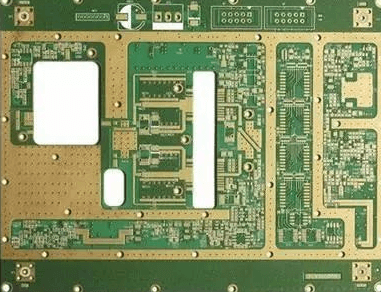
PCB wiring process requirements
1. line
Under normal circumstances, the signal line width is 0.3mm (12mil), the power line width is 0.77mm (30mil) or 1.27mm (50mil); the distance between the line-to-line and between the line and the pad is greater than or equal to 0.33mm (13mil In practical applications, consideration should be given to increasing the distance when conditions allow;
When the wiring density is high, it is considered (but not recommended) to use two lines between the IC pins. The width of the line is 0.254mm (10mil), and the line spacing is not less than 0.254mm (10mil). In special cases, when the device pins are denser and the width is narrower, the line width and line spacing can be appropriately reduced.
2. Pad (PAD)
The basic requirements for the pad (PAD) and the transition hole (VIA) are: the diameter of the disc is greater than the diameter of the hole is greater than 0.6mm; for example, universal pin resistors, capacitors and integrated circuits, etc., using the plate / hole size 1.6mm/0.8 Mm (63mil/32mil), sockets, pins and diodes 1N4007, etc., using 1.8mm/1.0mm (71mil/39mil). In practical applications, the size of the actual component should be determined. When conditions are available, the pad size can be appropriately increased.
The mounting hole diameter of the component designed on the PCB should be 0.2~0.4mm larger than the actual size of the component pin.
3. Via (VIA)
Typically 1.27mm/0.7mm (50mil/28mil);
When the wiring density is high, the size of the via hole can be properly reduced, but it should not be too small, consider using 1.0mm/0.6mm (40mil/24mil).
4. Pad, line, and via spacing requirements
PADandVIA: ≥0.3mm (12mil)
PADandPAD: ≥0.3mm (12mil)
PADandTRACK: ≥0.3mm (12mil)
TRACKandTRACK: ≥0.3mm (12mil)
When the density is high:
PADandVIA: ≥0.254mm (10mil)
PADandPAD: ≥0.254mm (10mil)
PADandTRACK: ≥0.254mm (10mil)
TRACKandTRACK: ≥0.254mm (10mil)
Fifth: wiring optimization and silk screen. “There is no best, only better!” No matter how hard you think about designing, after you finish drawing, look again and you will still feel that many places can be modified. The general design experience is: Optimize the wiring time is twice the time of the initial wiring. Feeling no place needs to be modified, you can lay copper (Place->polygonPlane). Copper is generally laid on the ground (note the separation of analog ground and digital ground), and power may also need to be laid when it is stacked. For screen printing, be careful not to be blocked by the device or removed by vias and pads. At the same time, when designing the components, the underlying word should be mirrored to avoid confusion.
Sixth: Network and DRC inspections and structural inspections. First of all, under the premise of determining that the circuit schematic design is correct, the generated network connection between the PCB network file and the schematic network file is checked (NET CHECK), and the design is corrected in time according to the output file results to ensure the wiring. The correctness of the connection relationship;
After the network inspection is properly passed, DRC inspection is performed on the PCB design, and the design is corrected in time based on the output file results to ensure the electrical performance of the PCB layout. Finally, the mechanical mounting structure of the PCB needs to be further checked and confirmed.
Seventh: plate making. Before this, it is better to have a review process.
PCB design is a mind-stricken work. Whose thoughts are high, experience is high, and the design of the board is good. Therefore, the design must be extremely careful, fully consider the factors in all aspects (such as easy maintenance and inspection of this item,