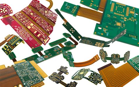
Aluminum substrate PCB production specifications and design rules
The main technical requirements are:
Size requirements, including board size and deviation, thickness and deviation, verticality and warpage; appearance, including requirements for cracks, scratches, burrs and delamination, aluminum oxide film, etc.; performance, including peel strength, surface resistivity, minimum breakdown voltage, dielectric constant, flammability and thermal resistance.
Special testing methods for aluminum-based copper-clad laminates:
First, the dielectric constant and dielectric loss factor measurement method, which is a variable Q value series resonance method, connecting the sample and the tuning capacitor in series to a high-frequency circuit to measure the Q value of the series circuit;
Second, the thermal resistance measurement method, which is calculated by the ratio of the temperature difference between different temperature measurement points to the heat conductivity. ?
II. Aluminum substrate circuit production
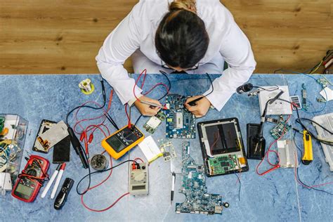
(1) Mechanical processing: Aluminum substrates can be drilled, but no burrs are allowed on the inner edge of the hole after drilling, which will affect the withstand voltage test. Milling the shape is very difficult. Punching the shape requires the use of advanced molds, and mold production requires a lot of skills, which is one of the difficulties of aluminum substrates. After the shape is punched, the edge must be very neat, without any burrs, and the solder mask layer on the edge of the board must not be damaged. Usually, a military mold is used, the holes are punched from the circuit, the shape is punched from the aluminum surface, and the force applied when punching the circuit board is shearing up and pulling down, etc. These are all skills. After punching the shape, the warpage of the board should be less than 0.5%.
(2) The aluminum base surface must not be scratched during the entire production process:
the aluminum base surface will change color or turn black when touched by hand or exposed to certain chemicals, which is absolutely unacceptable. Some customers will not accept re-polishing the aluminum base surface, so not scratching or touching the aluminum base surface during the entire process is one of the difficulties in producing aluminum substrates. Some companies use passivation technology, and some apply protective film before and after hot air leveling (tin spraying)… There are many tricks, and each has its own magical powers.
(3) Over-voltage test: Communication power aluminum substrates require 100% high-voltage testing.
Some customers require direct current, while others require alternating current. The voltage requirements are 1500V and 1600V, and the time is 5 seconds and 10 seconds. 100% of the printed circuit boards are tested. Dirt on the board surface, burrs on the edges of holes and aluminum substrates, line serrations, and any damage to the insulation layer will cause fire, leakage, and breakdown during the high-voltage test. Boards with delamination and blistering during the voltage test will be rejected.
III. Aluminum substrate PCB production specifications
- Aluminum substrates are often used in power devices with high power density, so the copper foil is relatively thick. If copper foil above 3oz is used, the etching process of thick copper foil requires engineering design line width compensation, otherwise, the line width after etching will be out of tolerance.
- The aluminum substrate of the aluminum substrate must be protected with a protective film in advance during the PCB processing process, otherwise some chemicals will corrode the aluminum substrate, resulting in damage to the appearance. And the protective film is very easy to be scratched, resulting in gaps, which requires the entire PCB processing process to be inserted.
- The hardness of the milling cutter used for the glass fiber board gong board is relatively small, while the hardness of the milling cutter used for the aluminum substrate is large. During the processing, the milling cutter speed of the glass fiber board is fast, while the speed of the aluminum substrate is at least two-thirds slower.
- The computer milling edge glass fiber board only uses the machine’s own cooling system to dissipate heat, but the processing of the aluminum substrate must be separately directed to the gong head.
IV. PCB process specifications and PCB design safety principles
- Purpose
Standardize the PCB process design of the product, specify the relevant parameters of the PCB process design, so that the PCB design meets the technical specifications of manufacturability, testability, safety, EMC, EMI, etc., and build the product’s process, technology, quality, and cost advantages in the product design process.
- Scope of application
This specification applies to the PCB process design of all electronic products, and is used for but not limited to PCB design, PCB board casting process review, single board process review and other activities.
If the contents of the relevant standards and specifications before this specification conflict with the provisions of this specification, this specification shall prevail.
- Definition
Via: A metallized hole used for inner layer connection, but it is not used to insert component leads or other reinforcing materials.
Blind via: A via that extends from the inside of the printed board to only one surface layer.
Buried via: A via that does not extend to the surface of the printed board.
Through via: A via that extends from one surface layer of the printed board to another surface layer.
Component hole: A hole used to fix component terminals to the printed board and electrically connect conductive patterns.
Standoff: The vertical distance from the bottom of the body of a surface-mounted device to the bottom of the pin.
- Reference standards or materials
TS-S0902010001《《Information Technology Equipment PCB Safety Design Specification》
TS-SOE0199001《《Electronic Equipment Forced Air Cooling Thermal Design Specification》
TS-SOE0199002《Electronic Equipment Natural Cooling Thermal Design Specification》
IEC60194《《Printed Circuit Board Design, Manufacturing and Assembly Terms and Definitions》》(Printed Circuit Board design
manufacture and assembly sembly-termsanddefiniTIons)
IPC-A-600F《Acceptably of printed board》
IEC60950
5.Specification content
5.1 PCB board requirements
5.1.1 Determine the board material and TG value used for PCB
Determine the board material selected for PCB, such as FR-4, aluminum substrate, ceramic substrate, paper core board, etc. If a board with a high TG value is selected, the thickness tolerance should be indicated in the document.
5.1.2 Determine the surface treatment coating of PCB
Determine the surface treatment coating of PCB copper foil, such as tin plating, nickel-gold plating or OSP, and indicate it in the document.
5.2 Thermal design requirements
5.2.1 High-heat devices should be considered to be placed at the air outlet or a location that is conducive to convection
Consider placing high-heat devices at the air outlet or a location that is conducive to convection in the PCB layout.
5.2.2 Higher components should be placed at the air outlet without blocking the air path
5.2.3 The placement of the heat sink should be conducive to convection
5.2.4 Temperature-sensitive devices should be kept away from heat sources
For heat sources with a temperature rise of more than 30°C, the general requirements are:
a. Under air cooling conditions, the distance between electrolytic capacitors and other temperature-sensitive devices and the heat source is required to be greater than or equal to 2.5mm;
b. Under natural cooling conditions, the distance between electrolytic capacitors and other temperature-sensitive devices and the heat source is required to be greater than or equal to 4.0mm.
If the required distance cannot be achieved due to space reasons, a temperature test should be performed to ensure that the temperature rise of the temperature-sensitive device is within the derating range.
5.2.5 Large area copper foil requires to be connected to the pad with insulation tape
To ensure good tin penetration, the pads of components on large area copper foil are required to be connected to the pads with insulation tape, for those that need to pass 5A
5..2.6 Symmetry of heat dissipation of pads at both ends of 0805 and chip components below 0805 after reflow
In order to avoid the phenomenon of deviation and tombstone after reflow, 0805 and chip components below 0805 after reflow. The pads at both ends should ensure heat dissipation symmetry, and the width of the connection between the pad and the printed conductor should not be greater than 0.3mm (for asymmetric pads)
5.2.7 Installation method of high-heat devices and whether to consider with a heat sink
Determine the installation method of high-heat devices to be easy to operate and weld. In principle, when the heat density of components exceeds 0.4W/cm3, the lead legs of the components and the components themselves are not enough to dissipate heat. Heat dissipation nets, bus bars and other measures should be used to improve the overcurrent capacity.
The legs of the bus bars should be connected at multiple points, and riveting should be used as much as possible after wave soldering or direct wave soldering to facilitate assembly and welding; for the use of longer bus bars, the PCB deformation caused by the mismatch between the thermal expansion coefficient of the heated bus bar and the PCB during wave soldering should be considered.
In order to ensure that tinning is easy to operate, the width of the tin channel should be no more than or equal to 2.0mm, and the spacing between the edges of the tin channel should be greater than 1.5mm.
5.3 Requirements for device library selection
5.3.1 The selection of existing PCB component package library should be confirmed
The selection of existing component library devices on PCB should ensure that the package is consistent with the physical outline, pin spacing, through-hole diameter, etc. of the components.
5.3.2 The PCB component package inventory of new devices should be confirmed
For devices that do not have a package library on PCB, a salvaged component package library should be established based on the device information, and the silk screen inventory should be guaranteed to be consistent with the actual object, especially whether the newly established component inventory of electromagnetic components, self-made structural parts, etc. is consistent with the component information (acknowledgement, drawings). New devices should establish a component library that can meet the requirements of different processes (reflow soldering, wave soldering, through-hole reflow soldering).
5.3.3 SMT devices that need to be wave soldered require the use of surface mount wave soldering pad library
5.3.4 The types of pin spacing of axial devices and jumpers should be as few as possible to reduce the molding and installation tools of the device.
5.3.5 Compatible devices with different PIN spacings should have separate pad holes, especially the compatible pads of package-compatible relays should be connected.
5.3.6 The pads of manganese copper wire and other jumpers used for measurement should be made non-metallized. If they are metallized pads, the resistor in the pad will be short-circuited after welding, and the effective length of the resistor will become smaller and inconsistent, resulting in inaccurate test results.
5.3.7 Surface mount devices cannot be used as manual welding debugging devices. Surface mount devices are easily damaged by thermal shock during manual welding.
5.3.8 Unless there is no problem in the experiment, pinless surface mount devices with a large difference in thermal expansion coefficient with PCB cannot be selected, which can easily cause pad pull-off.
5.3.9 Unless there is no problem in the experiment, non-surface mount devices cannot be selected as surface mount devices. Because this may require manual welding, the efficiency and reliability will be very low.
5.3.10 When copper plating is applied to the side of a multi-layer PCB as a soldering pin, it must be ensured that each layer is connected by copper foil to increase the adhesion strength of the copper plating. At the same time, there must be an experiment to verify that there is no problem. Otherwise, the copper plating on the side of the double-sided board cannot be used as a soldering pin.
5.4 Basic layout requirements
5.4.1 Reasonable PCBA processing procedures
The component layout of the finished board should ensure that the processing procedures of the finished board are reasonable, so as to improve the processing efficiency and pass rate of the finished board.
The processing flow selected for the PCB layout should maximize the processing efficiency.
5.4.2 The board feeding direction of the wave soldering process is required to be marked with silk screen
5.4.3 The BOTTOM side of the PCB that has been reflowed on both sides is required to have no large volume or too heavy surface mount devices. The weight limit of the first reflow soldering device is as follows:
A=device weight/contact area between pin and pad
Chip devices: A≦0.075g/mm2
Wing pin devices: A≦0.300g/mm2
J-shaped pin devices: A≦0.200g/mm2
Surface array devices: A≦0.100g/mm2
If there are overweight devices that must be placed on the BOTTOM side, the feasibility should be verified through experiments.
5.4.4 The safe distance for the back of the single board that needs wave soldering to avoid shadow effect has taken into account the distance of SMT components in the wave soldering process
5.4.5 For ceramic capacitors larger than 0805 package, try to place them close to the transmission edge or the area with less stress, and try to parallel the axial direction with the board feeding direction. Try not to use ceramic capacitors larger than 1825.
5.4.6 Try not to place SMD within 3mm around the frequently plugged-in and unplugged components or board edge connectors to prevent the stress generated when the connector is plugged-in and unplugged from damaging the components.
5.4.7 The standoff of the surface mount components that pass the wave soldering meets the specification requirements
The standoff of the surface mount components that pass the wave soldering should be less than 0.15mm, otherwise they cannot be placed on the B side for wave soldering. If the standoff of the component is between 0.15mm and 0.2mm, copper foil can be placed under the component body to reduce the distance between the bottom of the component body and the PCB surface.
5.4.8 The minimum safe distance for the back test points to not be connected to the solder during wave soldering has been determined
To ensure that there is no connection to the solder during wave soldering, the distance between the edges of the back test points should be greater than 1.0mm.
5.4.9 The pad spacing of the plug-in components through wave soldering is greater than 1.0mm
To ensure that there is no connection to the solder during wave soldering, the pad edge spacing of the plug-in components through wave soldering should be greater than 1.0mm (including the pad edge spacing of the component’s own pins).
It is preferred that the plug-in component pin spacing (pitch) is ≧2.0mm, and the pad edge spacing is ≧1.0mm.
5.4.10 No components within 3mm around BGA
To ensure maintainability, a 3mm no-layout area must be left around the BGA component, and a 5mm no-layout area is optimal. Generally, BGA is not allowed to be placed on the back (the first reflow soldering surface of a single board that has been reflowed twice); when there is a BGA component on the back, the component cannot be placed within the projection range of the 5mm no-layout area of the front BGA.
5.4.11 The minimum spacing between patch components meets the requirements
Same type devices: ≧0.3mm
Heterogeneous devices: ≧0.13*h+0.3mm (h is the maximum height difference of the surrounding adjacent components)
The distance requirement between components that can only be patched manually: ≧1.5mm.
5.4.12 The outer side of the component is greater than or equal to 5mm from the two board edges that are in contact with the through-board track
5.4.13 There should be enough space around adjustable and pluggable devices for debugging and maintenance. The arrangement direction and debugging space of the adjustable devices should be comprehensively considered according to the PCBA installation layout of the system or module and the debugging method of the adjustable devices; the space reserved around the pluggable device should be determined according to the height of the adjacent device.
5.4.14 All plug-in magnetic components must have a solid base, and plug-in inductors without bases are prohibited.
5.4.15 The pins of polar transformers should not be designed to be symmetrical as much as possible.
5.4.16 There are no components and traces in the forbidden area of the mounting hole (excluding the traces and copper foil of the mounting hole itself).
5.4.17 The distance between metal shell devices and metal parts and other devices meets safety requirements.
The arrangement of metal shell devices and metal parts should ensure that the distance from other devices meets safety requirements in space.
5.4.18 Requirements for layout of through-hole reflow devices
a. For PCBs with non-transmission side dimensions greater than 300mm, heavier devices should not be arranged in the middle of the PCB as much as possible to reduce the influence of the weight of the plug-in device on the deformation of the PCB during the welding process, and the influence of the plug-in process on the devices already placed on the board.
b. For easy insertion, the device
It is recommended to arrange the components close to the insertion operation side.
c. For components with longer dimensions (such as memory stick sockets, etc.), the length direction is recommended to be consistent with the transmission direction.
d. The distance between the edge of the through-hole reflow soldering pad and the QFP, SOP, connector and all BGA with pitch ≦ 0.65mm is greater than 10mm. The distance between other SMT components is > 2mm.
e. The distance between the through-hole reflow soldering body is > 10mm. There is no requirement for pin soldering with fixture support.
f. The distance between the edge of the through-hole reflow soldering pad and the transmission side is > 10mm; the distance from the non-transmission side is > 5mm.
5.4.19 Requirements for forbidden areas of through-hole reflow soldering components
a. Sufficient space should be left around the through-hole reflow soldering pad for solder paste coating. The specific forbidden area requirements are: for European connectors, there should be no components within 10.5mm from the board, and there should be no components and vias within the forbidden area.
b. The vias that must be placed in the forbidden area must be treated with solder mask plugging.
5.4.20 The layout of the device should take into account the interference of single board assembly as a whole. When designing the layout of the device, the assembly interference between single boards and single boards, single boards and structural parts should be considered, especially for high devices and single boards with three-dimensional assembly.
5.4.21 Distance requirements between devices and chassis
When laying out the device, try not to get too close to the chassis wall to avoid damaging the device when installing the PCB to the chassis. Pay special attention to the devices installed on the edge of the PCB, which will move slightly during impact and vibration or have no solid appearance: such as vertical resistors, baseless inductor transformers, etc. If the above requirements cannot be met, other fixing measures should be taken to meet safety regulations and vibration requirements.
5.4.22 Devices that have undergone wave soldering should be arranged at the edge of the PCB as much as possible to facilitate plugging. If the device is arranged at the edge of the PCB and the mounting fixture is well made, plugging of the hole is not even required during wave soldering.
5.4.23 When designing and laying out the PCB, the device should be allowed to undergo wave soldering as much as possible. When selecting components, try to select as few components that cannot be wave soldered as possible. In addition, the number of components placed on the soldering surface should be as small as possible to reduce manual soldering.
5.4.24 Bare jumpers cannot be placed on the board to cross the wires or copper foil on the board to avoid short circuits with the copper foil on the board. Green oil cannot be used as an effective insulation.
5.4.25 When laying out, all components should be easy to inspect and maintain after soldering.
5.4.26 The soldering end of the cable should be arranged as close to the edge of the PCB as possible for insertion and soldering, otherwise other components on the PCB will hinder the insertion and soldering of the cable or be knocked crooked by the cable.
5.4.27 For components with multiple pins on the same straight line, such as connectors, DIP package components, and T220 package components, the axis should be parallel to the wave soldering direction when laid out.
5.4.28 For lighter components such as diodes and 1/4W resistors, the axis should be perpendicular to the wave soldering direction when laid out. This can prevent the component from floating due to one end being soldered and solidified first during wave soldering.
5.4.29 There should be a certain space between the cable and the surrounding devices, otherwise the bent part of the cable will compress and damage the surrounding devices and their solder joints.
5.5 Routing requirements
5.5.1 Distance from the printed board to the board edge: V-CUT edge greater than 0.75mm, milling groove edge greater than 0.3mm.
In order to ensure that there is no copper exposure defect during PCB processing, all routing and copper foil are required to be away from the board edge: V-CUT edge greater than 0.75mm, milling groove edge greater than 0.3mm (the distance between the copper foil and the board edge should also meet the installation requirements).
5.5.2 There is no routing under the front of the radiator (or it has been insulated)
In order to ensure electrical insulation, there should be no routing around the bottom of the radiator (considering the offset and safety distance of the radiator installation). If it is necessary to run wiring under the radiator, insulation measures should be taken to insulate the radiator from the routing, or confirm that the routing and the radiator are at the same potential.
5.5.3 No wiring under the metal handle bar
To ensure electrical insulation, there should be no wiring under the metal handle bar.
5.5.4 Requirements for the prohibited area range of various screw holes
The prohibited area range of various specifications of screws (the range of this prohibited area is only applicable to the installation space that ensures electrical insulation, without considering the safety distance, and only applicable to round holes):
5.5.5 Increase the width of the isolated pad and the wiring connection part (teardrop solder), especially for the pad of the single-sided board, to avoid pulling the pad off during wave soldering.
5.6 Requirements for fixing holes, mounting holes, and vias
5.6.1 The mounting holes and positioning holes that need to be grounded on the upper and lower parts of the wave soldering board should be defined as right non-metallized holes.
5.6.2 The diameter of the via hole below BGA is 12mil
5.6.3 The minimum distance between the edge of the SMT pad and the edge of the via is 10mil. If the via is plugged with green oil, the minimum distance is 6mil.
5.6.4 There are no vias on the pads of SMT devices (Note: except for the pads of DPAK packages used for heat dissipation)
5.6.5 Normally, standard via hole sizes should be used
5.6.6 For boards that have been wave soldered, if there are devices mounted on the component surface, there should be no vias underneath or the vias should be covered with green oil.