PCB Design and Manufacturing: Key Insights for Success

Key Takeaways
In the realm of PCB design and PCB manufacturing, understanding the fundamentals is crucial for developing effective strategies that boost efficiency and ensure high-quality outputs. A solid grasp of basic principles, such as the role of electrical pathways, component placement, and thermal management, creates a solid foundation for tackling more complex challenges. When transitioning from design to PCB assembly, it is essential to adopt best practices that streamline processes. For instance, using automated assembly techniques can significantly reduce errors and improve consistency in production.
Moreover, investing in innovative technologies is becoming increasingly important. Techniques such as surface mount technology (SMT) enable smaller component sizes and greater circuit density which can enhance performance and lower costs. Coupled with advanced simulation software that allows for rigorous testing prior to production, these technologies are transforming traditional practices.
To further improve efficiency in PCB processes, one might consider integrating lean manufacturing principles which can help minimize waste and optimize resource use. Quality control measures should not be overlooked; implementing routine inspections at various production stages ensures product integrity and reliability in the final PCBA.
“Quality is not an act, it is a habit.” – Aristotle
Utilizing modern software tools plays an essential role in navigating today’s challenges in PCB design. These tools facilitate easier modifications during the design phase, allowing engineers to respond swiftly to any design flaws or customer feedback. Finally, being aware of future trends—such as increased miniaturization or IoT integration—can pave the way for groundbreaking developments in PCB production and ultimately lead to successfully completed projects that meet the market’s evolving demands.
Understanding the Fundamentals of PCB Design
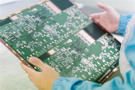
In the realm of electronics, PCB design is a critical component that serves as the backbone for electronic circuit functionality. A well-executed design allows for the efficient interconnection of various electronic components, facilitating smooth operation and reliability. The process begins with defining the circuit’s requirements, which includes determining the necessary components and their respective placements. This initial planning is vital, as it sets the groundwork for achieving optimal pcb assembly and ensures that pcba processes can be carried out without hitches.
Throughout the design phase, several fundamental aspects must be considered. One such aspect is signal integrity, which addresses how well signals can traverse through a PCB without interruptions or distortions. Designers must optimize traces, minimize lengths, and ensure proper grounding to maintain high-quality performance. Additionally, thermal management should not be overlooked; dissipating heat effectively prevents damage to sensitive components and prolongs their lifespan.
Another essential consideration is design for manufacturability (DFM). This principle entails creating designs that are easy to manufacture, reducing potential problems during pcb assembly. It often involves working closely with manufacturing teams to ensure that designs align with production capabilities. By combining all these elements—signal integrity, thermal considerations, and DFM—designers can lay a robust foundation for successful PCB manufacturing and subsequent implementation in various applications.
By understanding these core principles of PCB design, professionals can enhance their skills and contribute significantly to advancements in electronic production technologies.
Best Practices in PCB Manufacturing Techniques
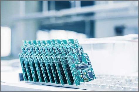
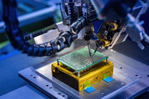
To achieve excellence in PCB manufacturing, it is imperative to adhere to a set of well-established best practices that ensure high-quality production. This begins with a thorough understanding of PCB assembly methods, where the integration of components onto the printed circuit board (PCB) is executed with precision. Engaging in advanced techniques such as surface mount technology (SMT) can enhance the overall efficiency of the assembly process while reducing space and costs. Additionally, maintaining a clean room environment minimizes contamination during manufacturing, which is crucial for ensuring that each component performs optimally within the overall pcba configuration. Quality checks at each stage of the process, right from design through production and final inspection, help to identify potential issues early and minimize defects. It’s also essential to leverage modern technologies, such as automated inspection systems, which can significantly augment the speed and accuracy of identifying flaws in the manufacturing process. By implementing these strategies, manufacturers not only improve yield rates but also contribute to producing reliable electronic products that meet customer expectations effectively.
Exploring Innovative Technologies in PCB Production
The landscape of PCB design and manufacturing is rapidly evolving, driven by innovative technologies that enhance productivity and quality. Among the forefront of these advancements is the integration of automated PCB assembly processes, which significantly reduce assembly time while improving precision. With the introduction of smart manufacturing systems, manufacturers can utilize data analytics to optimize workflows and minimize waste.
Incorporating additive manufacturing technologies, such as 3D printing, into PCBA (Printed Circuit Board Assembly) has revolutionized prototyping and custom design capabilities. This allows for rapid iterations and more creative freedom in design stages. Moreover, advancements in materials science have led to the development of high-performance substrates that improve signal integrity and thermal management—key factors in modern electronics efficiency.
Below is a summary table highlighting some of the innovative technologies currently shaping PCB production:
| Technology | Description | Benefits |
|---|---|---|
| Automated Assembly | Utilizes robotics to perform repetitive assembly tasks | Increases speed, reduces human error |
| Additive Manufacturing | 3D printing technologies for rapid prototyping | Enables custom design solutions |
| Advanced Materials | High-performance substrates for better signal integrity | Enhances compatibility with high-frequency applications |
| Data Analytics | Real-time analysis for process optimization | Reduces waste and improves operational efficiency |
These technological innovations not only strengthen the production process but also set new standards in the industry for quality and performance of final products. As we navigate this ever-evolving landscape, it becomes crucial for PCB designers and manufacturers to stay abreast of these trends to leverage their potential fully. Understanding how these elements interact will be key to sustaining competitive advantage in PCB manufacturing and assembly.
Strategies for Enhancing Efficiency in PCB Processes
Enhancing efficiency in PCB processes is crucial for organizations striving to remain competitive in the ever-evolving electronics industry. One effective strategy is to optimize design protocols by incorporating automated tools during the PCB design phase. Such tools not only reduce human error but also expedite the transition from design to prototype, thereby making the pcb assembly process smoother. Moreover, adopting a lean manufacturing approach can significantly minimize waste and bottlenecks in production. Establishing robust communication channels between teams involved in designing and manufacturing can lead to faster resolutions of issues arising during pcba production. Another pivotal strategy involves utilizing advanced materials that offer better performance and reliability; this decision can markedly enhance the final product’s quality while maintaining cost-effectiveness. Regularly reviewing and updating the supply chain management processes ensures that materials are sourced efficiently, contributing further to enhanced production timelines and reduced lead times. Additionally, implementing continuous training programs for employees tackles skill gaps and fosters a culture of innovation within the team. Collectively, these strategies form a comprehensive approach towards improving workflow efficiency and augmenting overall productivity in PCB processes.
Quality Control Measures in PCB Design and Manufacturing
In the realm of PCB design and manufacturing, ensuring the integrity and reliability of the final product is paramount. Quality control measures encompass a range of practices aimed at maintaining high standards throughout the entire process. These measures begin at the very outset, during the design phase, where it’s crucial to employ robust design rules that can help prevent potential issues during later stages such as PCB assembly. Stakeholders should consider implementing simulation tools that allow designers to visualize performance and catch flaws before proceeding to production.
As the manufacturing process advances, rigorous inspections should be established at critical checkpoints. For instance, during PCBA (Printed Circuit Board Assembly), visual inspections and automated optical inspection (AOI) systems can effectively identify defects such as insufficient solder or misplaced components. Additionally, regular audits of manufacturing facilities help ensure compliance with industry standards and foster a culture of continuous improvement.
A strong emphasis on documentation is also necessary; maintaining clear records enables teams to trace defects back to their source quickly, thereby avoiding future errors. Moreover, fostering communication between design engineers and manufacturing personnel can enhance understanding around tolerance levels and material choices, thereby minimizing discrepancies.
Ultimately, integrated quality assurance practices not only enhance the efficiency of PCB processes, but they also significantly impact customer satisfaction through improved product reliability and performance in real-world applications. By prioritizing these quality control measures, organizations can navigate the complexities of PCB design and manufacturing while positioning themselves as leaders in a competitive market.

The Role of Software Tools in Modern PCB Design
In today’s rapidly evolving electronics landscape, software tools play a pivotal role in PCB design and pcb assembly processes. These tools enhance the efficiency of PCBA by enabling designers to create intricate layouts and intricate circuit patterns with improved accuracy. The integration of software solutions allows for real-time collaboration among teams, significantly reducing the time it takes to move from concept to production. Advanced simulation software enables designers to test circuits virtually before physical prototypes are created, helping to identify potential issues early in the design phase. Furthermore, managing data through these tools streamlines changes and revisions, ensuring that all stakeholders are aligned during the production process. As technology continues to advance, the impact of software on PCB design will likely expand, incorporating features such as artificial intelligence that can predict design flaws and optimization opportunities. Thus, leveraging these modern PCB design tools is crucial for achieving high-quality outcomes in pcb manufacturing and ensuring that the final products meet performance expectations effectively.
Future Trends in PCB Manufacturing and Design
As the electronics industry continues to evolve, future trends in PCB manufacturing and design are becoming increasingly dynamic. One key trend is the growing emphasis on miniaturization. As electronic devices become smaller and more compact, the demand for advanced pcb assembly techniques is on the rise. This trend necessitates innovative design strategies that can accommodate higher component densities without compromising functionality or performance. Another significant development is the integration of smart technologies into PCB processes, enabling enhanced monitoring and automation during manufacturing. The incorporation of Artificial Intelligence and Machine Learning can streamline operations, predict maintenance needs, and improve overall quality control in pcba production.
Moreover, sustainability is emerging as a critical focus in PCB design and manufacturing. Companies are increasingly adopting eco-friendly materials and processes to minimize their environmental impact. This shift towards sustainable practices aligns with consumer expectations for greener products and can lead to cost savings through more efficient resources utilization.
The rise of 5G technology also presents new challenges and opportunities for PCB manufacturers. As networks expand, the demand for high-frequency PCBs that can efficiently handle increased data throughput will require significant innovation in both design techniques and materials utilized.
In summary, keeping pace with these emerging trends will be essential for companies seeking to maintain a competitive edge in the rapidly evolving landscape of electronics production. Adapting to changes in technology, market demands, and regulatory standards will shape the future of PCB design and manufacturing as a whole.

Case Studies: Successful PCB Projects and Lessons Learned
In the realm of PCB design and manufacturing, real-world examples often provide invaluable insights into best practices and potential pitfalls. Successful projects illustrate how effective planning, collaboration, and innovation can lead to exceptional outcomes. For instance, one notable case involved a tech startup that successfully launched a new consumer electronics product utilizing streamlined pcba processes. By prioritizing modularity in their PCB assembly, they were able to reduce production time significantly while maintaining high standards of quality. Another compelling example is an automotive company that embraced advanced PCB manufacturing techniques to enhance the pcba for critical safety features in their vehicles. They implemented rigorous quality control measures, coupled with automated inspection technologies, to ensure error-free production. These projects highlight the importance of integrating innovative methodologies and robust testing protocols in the design and manufacturing phases. Moreover, they underscore the necessity of cross-functional teamwork where engineers work closely with manufacturing teams to troubleshoot issues early in the process. By analyzing these successful cases, other organizations can glean lessons on optimizing their own PCB design strategies and improving efficiencies in their manufacturing processes for future success.
Conclusion
In the intricate world of PCB design and manufacturing, understanding the nuances of pcb assembly and pcba processes is paramount for achieving excellence. The journey from conceptualization to the actualization of a printed circuit board is filled with challenges that require precision, innovation, and adherence to best practices. By integrating cutting-edge technologies and robust strategies, manufacturers can significantly enhance efficiency in their production lines, thereby ensuring top-tier quality. Moreover, implementing rigorous quality control measures fosters a culture of continuous improvement and reliability in output. As the industry evolves, staying abreast of emerging trends and investing in versatile software tools for modern design will be vital in navigating the complexities of PCB production. Ultimately, success in this field hinges on an organization’s ability to adapt and innovate while maintaining a keen focus on the essentials of pcb assembly techniques and practices. This holistic approach not only maximizes productivity but also positions businesses advantageously in an increasingly competitive landscape.
FAQs
What is PCB assembly and how does it relate to the manufacturing process?
PCB assembly, often abbreviated as PCBA, is the process of placing components onto a printed circuit board (PCB), which is a crucial step in the overall PCB manufacturing process. It combines various elements such as soldering, testing, and inspection to ensure that the final product operates effectively.
What are the main steps involved in PCB assembly?
The main steps typically include designing the PCB, fabricating it, assembling components onto the board, soldering those components in place, and finally testing to ensure quality and performance. Each of these stages is essential to deliver a reliable end product.
What technologies are used in modern PCB assembly?
Modern PCB assembly utilizes advanced techniques such as surface-mount technology (SMT), automated optical inspection (AOI) systems, and robotic assembly processes. These innovations greatly enhance speed and precision while reducing the risk of errors.
How does quality control impact PCB assembly outcomes?
Quality control measures play a vital role in PCB assembly, ensuring that every unit meets specified standards. This includes conducting thorough inspections at various stages of production and implementing rigorous testing protocols to catch defects early.
Why is efficiency important in PCB manufacturing processes?
Efficiency in PCB manufacturing translates to cost savings, faster turnaround times, and improved output quality. By optimizing every aspect of production—from design through PCBA—manufacturers can enhance their overall competitiveness in the market.