Efficient Techniques for Stencil PCB Assembly Explained
Key Takeaways
Understanding stencil PCB assembly is crucial for anyone involved in PCB manufacturing. This process allows for the precise application of solder paste onto circuit boards, which is critical for successful soldering in PCBA. Key techniques to enhance precision include the selection of appropriate stencil thickness, which can significantly impact the paste deposit size and overall solder joint quality. Additionally, the correct alignment of the stencil to the PCB during placement ensures minimal wastage and optimal paste coverage.
Utilizing best practices such as thorough cleaning of stencils can prevent contamination that might lead to defects in the final product. Innovative approaches, such as using laser-cut stencils or incorporating advanced materials, can further boost accuracy and efficiency in stencil PCB assembly.
Here’s a concise comparison of traditional versus innovative stencil techniques:
| Technique | Traditional Methods | Innovative Methods |
|---|---|---|
| Stencil Material | Steel or Mylar | Laser-cut or polyimide |
| Application | Manual or semi-automatic | Fully automated processes |
| Precision Level | Moderate | High |
The future trends in PCB assembly point towards increased automation, which not only enhances efficiency but also supports higher scalability in production runs. By focusing on these techniques and best practices, manufacturers can significantly streamline their PCBA processes while maintaining high levels of quality and reliability.
Introduction to Stencil PCB Assembly
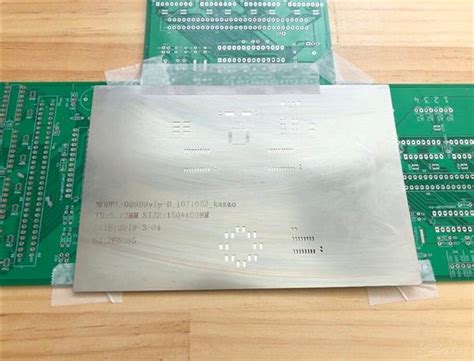
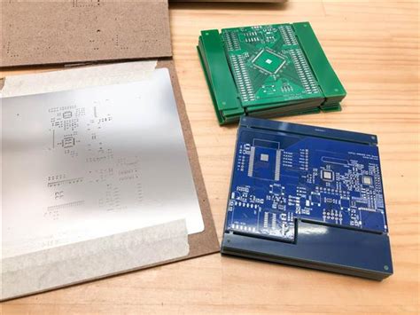
Stencil PCB assembly is a crucial process in the realm of electronics, where the accurate placement of components on a printed circuit board (PCB) is essential for functionality and reliability. This method involves using a stencil to deposit solder paste onto specific areas of the PCB, effectively preparing it for the placement of electronic components. The application of solder paste must be precise; otherwise, it can lead to defects in the final assembly, impacting both performance and service life. By utilizing proper stenciling techniques, manufacturers can significantly enhance the quality and efficiency of their PCBA processes. This practice not only ensures that solder is applied uniformly but also reduces wastage and rework associated with improper application. Moreover, careful selection of stencil materials and designs can contribute to improved thickness control and enhanced adherence to component pads, thereby optimizing the overall assembly process. As technology advances, understanding the nuances of stencil PCBA becomes increasingly important for companies striving to maintain competitive manufacturing standards while ensuring efficiency and effectiveness in their production lines.
Key Techniques for Enhancing Precision
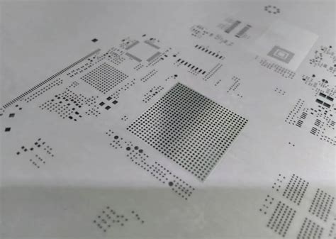
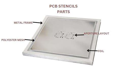
Precision in stencil PCB assembly is vital for ensuring the functionality and reliability of electronic devices. One of the primary techniques to achieve this is the careful design of the stencil itself. The openings in the stencil should be tailored to match the specific component sizes and solder paste requirements of your PCB assembly (pcba). Additionally, maintaining an optimal thickness of the stencil can significantly influence solder paste deposit volumes, which directly impacts solder joint quality.
Another critical approach is to utilize a robust squeegee technique during the application process. The angle, pressure, and speed should be calibrated to reduce paste bridging between pads and ensure consistent volume across all pads. Implementing a vacuum assist during stencil removal can further enhance precision by minimizing the risk of smearing or misalignment.
Moreover, conducting thorough inspection processes using automated optical inspection (AOI) systems can help detect any discrepancies in pasting accuracy before proceeding to subsequent steps in your PCB assembly workflow. By adopting these industry best practices, manufacturers can greatly improve yield rates while maintaining high standards of precision necessary for advanced electronic applications. Each element contributes significantly to achieving optimal results in stencil PCB assembly, ultimately leading to enhanced product performance and reliability.
Best Practices for Efficient PCB Assembly
In the world of stencil PCB assembly, implementing best practices is crucial to achieving both precision and efficiency in the PCBA process. One of the foundational strategies is to ensure that you utilize high-quality stencils that are compatible with your specific requirements. A well-designed stencil not only enhances solder paste application but also minimizes potential defects during assembly. Moreover, it’s essential to maintain a clean working environment; regular cleaning and maintenance of both stencils and printing equipment can significantly improve paste transfer efficiency and reduce contamination-related issues. Another critical aspect involves the optimization of the solder paste itself; using the right viscosity and composition tailored to your PCB’s design can make a notable difference in the final product quality. Additionally, training your team on the best handling practices for components will reduce the risk of damage and misalignment during placement, ultimately facilitating a smoother PCB assembly operation. Lastly, creating a robust feedback loop by analyzing yield rates and identifying areas for improvement will ensure that your processes remain adaptable and effective in meeting evolving manufacturing standards.
Innovative Approaches to Stencil Design
In the rapidly evolving field of pcb assembly, innovative approaches to stencil design play a crucial role in enhancing both efficiency and precision. One effective method is the use of laser-cut stencils, which provide high accuracy in paste application, ensuring that solder paste deposits are evenly distributed across the PCB. This technique reduces the potential for defects during the pcba process, leading to higher yield rates and less rework.
Another advancement is the integration of 3D printing technology in stencil production. This allows for rapid prototyping and the ability to create custom stencils tailored for specific PCB layouts. With this technique, engineers can experiment with various designs without committing significant resources, giving them the flexibility to optimize stencil parameters quickly.
Moreover, employing automated stencil cleaning systems has dramatically improved operational efficiency. These systems ensure that stencils are kept in optimal condition by removing excess solder paste between uses. Clean stencils contribute not only to improved pcb assembly outcomes but also extend their lifespan, resulting in cost savings over time.
Lastly, data-driven design optimization through simulation software enables engineers to analyze different solder paste deposition strategies before actual production begins. By leveraging this innovative software, manufacturers can pinpoint potential issues related to paste volume and distribution early in the design phase, paving the way for seamless transitions into full-scale production. In conclusion, embracing these innovative approaches can significantly advance stencil PCB assembly processes, leading to superior results and competitive advantages in the marketplace.
Troubleshooting Common Issues in Stencil PCB Assembly
In the intricate world of pcb assembly, challenges are bound to arise, impacting both efficiency and output quality during the stencil PCBA process. One prevalent issue is misalignment during the printing stage, which can lead to solder paste application errors. To address this, it is crucial to ensure that both the stencil and the printed circuit board are accurately registered before beginning the stencil process. Utilizing high-precision equipment can significantly reduce alignment discrepancies. Additionally, another common concern involves inconsistent solder paste deposit volumes. This issue often stems from the choice of stencil thickness and aperture design. It’s important to select an appropriate stencil that complements the specific requirements of the component being used, thus promoting a more optimized deposit output. Furthermore, contamination on either the stencil or PCB surface can result in defective assemblies. Regular cleaning schedules and using high-quality materials in pcb assembly can mitigate this risk significantly. By identifying and resolving these common issues early on, manufacturers can enhance both productivity and overall quality control measures in their PCBA processes, leading to more reliable electronic products in the market.
The Role of Automation in Stencil PCB Processes
Automation has become a pivotal factor in enhancing the pcb assembly process, particularly in stencil application. By integrating advanced technologies into pcba operations, manufacturers can achieve unparalleled levels of accuracy and efficiency. Automated stencil printing systems utilize high-precision machinery that consistently applies solder paste to the PCB, ensuring uniformity across all components. This reduces the risk of human error, which is common in manual processes. Moreover, automated systems can easily adapt to different designs and layouts, setting up quickly for various production runs without compromising quality. The implementation of automation not only streamlines workflow but also allows for real-time monitoring and adjustments, significantly improving production speed while maintaining high-quality standards. Additionally, combining automation with data analytics enables manufacturers to predict issues before they arise, further enhancing the overall pcb assembly process. As a result, the role of automation serves as a cornerstone for modern pcba methodologies, driving advancements that optimize efficiency and precision in stencil PCB tasks.
Future Trends in PCB Manufacturing Techniques
As technology continues to evolve, the pcb assembly industry is witnessing significant transformations, particularly in the adoption of advanced methodologies. One such trend is the integration of automation within stencil processes, which not only enhances efficiency but also improves accuracy in pcba. Companies are increasingly turning to automated systems that streamline various stages of production, limiting human error and ensuring consistency in quality. Furthermore, the rise of smart manufacturing solutions is facilitating real-time monitoring of the assembly process, allowing for immediate adjustments based on data-driven insights. The emergence of hybrid techniques that combine traditional stencil methods with innovative tools is also on the rise. These approaches enable manufacturers to achieve more complex designs without compromising on speed or precision. Additionally, advancements in materials technology are leading to better solder paste formulations which enhance adhesion and reliability in connections. As these trends unfold, the future of stencil PCB assembly looks promising, with opportunities for further optimization and enhanced performance across various applications. Embracing these innovations will be pivotal for companies looking to stay competitive in the ever-evolving landscape of electronics manufacturing.
Conclusion
In summary, stencil PCB assembly stands as a pivotal technique in the realm of PCB manufacturing. The adoption of effective techniques such as utilizing precision alignment tools and implementing automated processes can significantly enhance the accuracy and efficiency of PCBA. By streamlining the application of solder paste with stencils, manufacturers can reduce waste and improve yield rates. Furthermore, adhering to best practices—like regular maintenance of stencils and careful inspection—ensures that the assembly process remains smooth and effective. As innovative approaches to stencil design continue to emerge, they promise to further optimize the PCB assembly workflow by minimizing defects and maximizing throughput. Embracing these strategies not only meets current industry demands but also prepares manufacturers for the evolving challenges in the realm of PCBA. With automation playing a critical role in modern stencil processes, it is evident that investing in advanced technologies will provide a competitive edge in the ever-demanding world of electronics production. As we move forward, staying informed about future trends will be essential for achieving sustained success in stencil PCB assembly.
FAQs
What is stencil PCB assembly and why is it important?
Stencil PCB assembly is a process that utilizes a thin sheet of material with openings that correspond to the components on a PCB. This technique allows for the precise application of solder paste to the surfaces of the board, significantly enhancing the accuracy and efficiency of PCBA.
What are common techniques used in stencil PCB assembly?
Common techniques include laser cutting for creating stencils, automated stencil printing, and inspection methods post-assembly. Each method plays a vital role in ensuring consistent quality in pcb assembly.
How do I choose the right stencil for my PCB?
The right stencil depends on factors such as the type of components used in your design, the pitch of those components, and your manufacturing capabilities. It’s crucial to select a stencil that will allow optimal paste deposition to ensure successful PCBA.
What troubleshooting methods can I apply during stencil PCB assembly?
Troubleshooting can involve checking for inconsistencies in solder paste application, inspecting the stencils for wear or damage, and ensuring alignment between components and pads on the PCB. Regular maintenance of equipment also plays a crucial role.
How does automation improve stencil PCB assembly processes?
Automation increases speed and precision, minimizes human error, and enhances repeatability in producing high-quality assemblies. Implementing automation can streamline operations within your pcb assembly, driving efficiency and reducing labor costs.