How to lay out the digital ground and analog ground in circuit design?
The reason why digital ground and analog ground affect each other is not because one is called digital and the other is called analog, but because they use the same elevator: ground, and the shaft used by this elevator is the ground line laid on the PCB.
In the design of high-speed PCB, the interference problem in the PCB design of digital-analog mixed circuits has always been a difficult problem.
In particular, analog circuits are generally the source of signals, and whether they can correctly receive and convert signals is an important factor to be considered in PCB design.
This article analyzes the mechanism of interference generation in mixed circuits, combines design practice, explores the general processing methods of mixed circuits, and verifies it through design examples.
Printed circuit boards (PCBs) are the support for circuit elements and devices in electronic products, and they provide electrical connections between circuit elements and devices. Now many PCBs are no longer single-function circuits, but are composed of a mixture of digital circuits and analog circuits. Data is generally collected and received in analog circuits, while bandwidth and gain must be digitized to be controlled by software, so digital circuits and analog circuits often exist on the same board at the same time, and even share the same components.
Considering the mutual interference between them and the impact on circuit performance, the layout and wiring of the circuit must have certain principles.
The special requirements for power transmission lines in mixed-signal PCB design and the requirements for isolating noise coupling between analog and digital circuits increase the complexity of layout and wiring during design. Here, by analyzing the layout and wiring design of high-density mixed-signal PCB, the required PCB design goals can be achieved.
Generation mechanism of interference in mixed analog and digital circuits
Compared with digital signals, analog signals are much more sensitive to noise, because the operation of analog circuits depends on continuously changing currents and voltages, and any slight interference can affect its normal operation, while the operation of digital circuits depends on the detection of high or low levels at the receiving end according to pre-defined voltage levels or thresholds, and has a certain anti-interference ability.
However, in a mixed signal environment, digital signals are a noise source relative to analog signals.
When digital circuits are working, there are only two stable effective voltages: high and low voltages. When the digital logic output changes from high voltage to low voltage, the ground pin of the device will discharge and generate switching current, which is the switching action of the circuit.
The faster the digital circuit is, the shorter its switching time is generally required.
When a large number of switching circuits change from logic high to logic low at the same time, due to the insufficient ability of the ground line to pass current, a large amount of switching current will cause the logic ground voltage to fluctuate, which we call ground bounce. As shown in Figure 1. The ground bounce noise and power supply disturbance caused by the digital circuit, if coupled to the analog circuit, will affect the working performance of the analog circuit. Since a considerable number of interference sources are generated through the power supply and ground bus, among which the noise interference caused by the ground line is the largest, the design of the ground and power supply is particularly important during PCB design.
How to lay the digital ground and analog ground in circuit design?
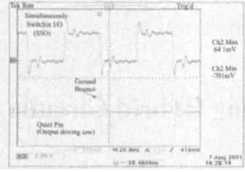
Figure 1 Ground bounce noise
General processing principles for PCB design of digital-analog mixed circuits
The above describes the generation mechanism of mixed circuit interference, so how to reduce the mutual interference between digital signals and analog signals?
Before designing, you must understand the two basic principles of electromagnetic compatibility (EMC):
The first principle is to reduce the area of the current loop as much as possible. If the signal cannot return through the smallest possible loop, it may form a large loop antenna. The second principle is that the system uses only one reference plane. On the contrary, if the system has two reference planes, a dipole antenna may be formed. These two situations should be avoided as much as possible in the design.
(1) Layout and wiring principles.
The first factor to be considered in the layout of components is to separate the analog circuit part from the digital circuit part. The analog signal is routed in the analog area of all layers of the circuit board, while the digital signal is routed in the digital circuit area. In this case, the return current of the digital signal will not flow into the ground of the analog signal.
For some high-frequency lines with special requirements, it is best to manually route them, and use differential lines or shielded lines when necessary. Sometimes due to the location of the input/output connector, the routing of digital and analog circuits must be mixed together, which is likely to cause mutual influence between the analog and digital circuits.
This requires avoiding routing digital clock lines and high-frequency analog signal lines near the analog power layer, otherwise the noise of the power signal will be coupled into the sensitive analog signal. To try to achieve a low-impedance power and ground network, the inductive reactance of the digital circuit wires should be minimized and the capacitive coupling of the analog circuit should be minimized. Digital circuits have high frequencies and analog circuits have high sensitivity. For signal lines, high-frequency digital signal lines should be as far away from sensitive analog circuit devices as possible.
(2) Power and ground processing.
In the design of complex hybrid circuit boards, the layout and processing of ground lines are important factors in improving circuit performance. Some people suggest separating the digital ground and analog ground on mixed-signal circuit boards to achieve isolation between the digital ground and analog ground. However, this method often crosses the split gap for wiring, which will cause a sharp increase in electromagnetic radiation and signal crosstalk.
Understanding the path and method of current return to the ground is the key to optimizing the design of mixed-signal circuit boards. If the ground line layer must be split and the wiring must be passed through the gap between the splits, a single-point connection can be made between the split grounds to form a bridge between the two grounds, and then wiring can be done through the bridge, as shown in Figure 2.
How should digital and analog grounds be laid out in circuit design?
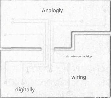
Figure 2 Schematic diagram of ground plane splitting by the bridge method
In this way, a direct current return path can be provided under each signal line, or optical isolation devices, transformers, etc. can be used to achieve signal crossing the split gap. However, in actual work, PCB design tends to adopt a unified ground.
By partitioning digital circuits and analog circuits and appropriate signal routing, some difficult layout and routing problems can usually be solved, and at the same time, some potential troubles caused by ground segmentation will not occur. By comparing the test results of the circuit board, it can be found that the unified ground solution is superior to the segmented ground in terms of function and EMC performance.
There are usually independent digital and analog power supplies on mixed-signal PCB boards.
A split power plane should be used, preferably close to and below the ground plane. The power plane may couple radio frequency current to the circuit that can be attached in space. In order to reduce this coupling effect, the power plane is required to be physically 20H smaller than the adjacent ground plane (H refers to the distance between the power supply and ground plane layers).
(3) Processing of hybrid devices.
Common hybrid devices include crystal oscillators, high-speed A D devices, etc., which have both digital circuits and analog circuits inside the device. Generally, the AGND and DGND pins are connected to the same low-impedance analog ground plane externally, and the leads are required to be as short as possible. Any additional impedance of DGND will couple more digital noise into the analog circuit inside the device through parasitic capacitance.
Of course, this will cause the digital current inside the converter to flow into the analog ground plane, but this will cause much less interference than connecting the DGND pin of the converter device to the noisy digital ground plane. Like grounding, the analog and digital power pins should also be connected to the analog power plane, and appropriate bypass capacitors should be connected as close to each power pin as possible. If necessary, the analog power pins should be isolated from the digital power pins by means of jumper inductors.
Hybrid circuit PCB design is a complex process. The layout and wiring of components and the processing of power and ground lines will directly affect the circuit performance and electromagnetic compatibility performance. Certain wiring rules must be followed during design to ensure that the designed PCB board meets the design requirements.