AI servers give rise to innovative changes, and the electronics industry faces a new round of product quality challenges
Driven by factors such as the surge in AI demand, the 5G upgrade cycle, and the intelligent electrification of automobiles, the global electronics market has entered a new round of growth, especially in the fields of communications electronics, consumer electronics, and automotive electronics. While demand growth has prompted upstream capacity upgrades, it has also brought stricter standards in manufacturing and design, and the tolerances that various electronic components can tolerate have been reduced from millimeters to nanometers.
Against this background, on May 22, Zeiss will hold the “Zeiss, ‘Quality’ Respects Tomorrow” ZEISS Quality Innovation Days China Online Summit Electronics Industry Theme Day event, together with opinion leaders and technical experts from well-known companies such as Hi-P Group, TE, and Precision Technology, to discuss the pain points of the electronics industry in quality control, and share and display innovative quality solutions for the electronics industry.
Starting from May 20, World Metrology Day this year, the five-day “Zeiss, ‘Quality’ Respects Tomorrow” ZEISS Quality Innovation Days China Online Summit will start with five industry theme days: new energy vehicles, medical, electronics, power and energy, and die-casting. You can participate by visiting the Zeiss official website or the Zeiss Industrial Quality Solutions WeChat public account. We look forward to your joining the quality event.
Challenges of high-layer PCB board detection driven by AI
With the popularity of various AI accelerators such as GPU and NPU in data centers, high-layer PCB boards are widely used to ensure the scalability of computing power and high-speed communication, and the number of layers is increasing year by year. Now the number of PCB layers of AI servers has reached more than 20 layers. With the trend of cloud service providers and data centers continuing to expand AI computing power, high-layer PCB boards not only usher in massive orders, but also put forward higher requirements for PCB technology.
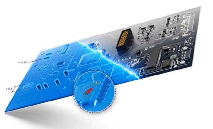
For high-layer PCB boards, the production technology itself is more difficult. Compared with conventional PCB boards, the boards are thicker, the number of layers is more, the line density is higher, the vias are denser, and the inter-layer alignment and reliability requirements are also higher. This also leads to the need to use a microscope to check the surface defects of the circuit board in order to ensure the yield of high-layer PCB boards. Zeiss provides an electron microscope solution that can detect micron-level/nano-level defects and complete the measurement of parameters such as blind hole depth, plating height, and surface roughness of PCB boards.
At the same time, as the area of AI server PCB boards becomes larger and larger, higher requirements are also placed on the size of the test pieces that the testing equipment can support. Zeiss will also launch new testing equipment on the theme day of the electronics industry at the “Zeiss, ‘Quality’ for Tomorrow” online summit, which can easily realize the surface defect detection of large-size AI server PCB boards.
Quality assurance of high-speed connectors
In data centers, high-speed communications have also promoted connectors into a new round of technological innovation. As Ethernet moves towards 800G and 1.6T, the maximum speed of SerDes has developed from 56G to 224G required for high-speed Ethernet. In addition, as the density between data center infrastructure continues to increase, the connection between internal components of the equipment is becoming more and more compact, and the volume requirements of connectors are becoming smaller and smaller. In order to increase the connection density of the network and give full play to the efficiency of AI hardware computing power, the key to breaking the interconnection bottleneck lies in high-speed connectors.
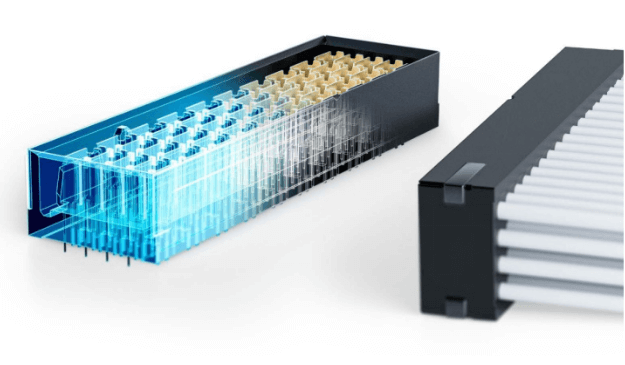
From the initial casting to the final assembly, connector manufacturers need to achieve more accurate measurement and dimensional quality control while achieving batch screening. In the mold development stage of new connectors, with the help of Zeiss’s metrological industrial CT scanning products, the mold repair time can be reduced through reverse engineering. To ensure that the connector pins are aligned and the size meets the standard, the Zeiss three-coordinate measuring machine can be used to effectively control the size and position tolerance.
Smartphones are developing telephoto lenses, and higher optical module precision requirements are required
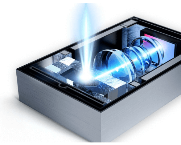
As the smartphone market becomes saturated, most manufacturers have carried out differentiated designs on cameras, such as telephoto and super telephoto cameras, in order to further improve user demand for phone replacement. Lens modules with longer focal lengths often mean increased length, which makes it more challenging to put them inside thin and light phones, especially folding screen phones.
Take the periscope telephoto lens equipped with the new generation of flagship smartphones as an example. Multiple reflector groups are used in a limited space to extend the optical path and achieve a telephoto effect. As for anti-shake and autofocus, they rely on OIS optical anti-shake components and autofocus structures to move CMOS left and right and front and back. In a small-size CMOS camera module, even a slight movement error will lead to a reduction in image quality, which places extremely high demands on the accuracy, resolution and repeatability of the measurement system.
Facing this detection challenge, Zeiss PRISIMO three-dimensional coordinate measuring machine and CALYPSO provide a complete solution, which accurately reflects the actual size after assembly by simulating the moving trajectory of ceramic balls moving in structural parts. For more innovative quality solutions in the electronics industry, please visit the “Zeiss, ‘Quality’ Respects Tomorrow” Online Summit.
Precision assembly of Pancake VR equipment
The optical modules of emerging XR devices also put forward higher requirements for assembly. Taking the current mainstream Pancake VR head display device as an example, compared with the previous generations of Fresnel structure, the Pancake architecture significantly reduces the thickness of the device and uses multi-layer optical film products to extend the optical path by folding the optical path with the help of various polarizers. For this reason, the assembly and alignment between optical modules are very important, otherwise the image quality will be affected by errors. Not only that, because the Pancake optical module uses multi-material hybrid components, traditional CT scanning is likely to produce artifacts, affecting the measurement results.
The industrial CT measuring machine provided by Zeiss provides high-precision and high-resolution scanning, quickly checks the gap between the lens and the edge of the lens and the thickness of the lens multilayer optical film, and accurately measures the assembled Pancake optical module without destroying the sample. In conjunction with AMMAR (Advanced Hybrid Material Artifact Reduction) in the Zeiss scatterControl module, artifacts in the measurement results can be effectively reduced.
XR devices also have a type of accessories that are often overlooked, namely input devices such as handles. In order to achieve ergonomic design and reduce fatigue from long-term hand-holding, customers have high requirements for the flatness, gap and repeatability of the surface contour when designing such devices, so accurate structural part contour detection is required.
At the same time, for the sake of lightness, the outer wall of such equipment is usually thinner, which is more prone to deformation and deviation. Therefore, in defect detection, the use of non-contact three-dimensional coordinate measuring machines can avoid the equipment from being subjected to force while not leaving any dead corners. The Zeiss METROTOM CT series provides excellent accuracy, while greatly reducing scanning time and improving detection efficiency.
Zeiss provides customers with reliable solutions with its rich expertise in the electronics industry. High-precision hardware and easy-to-use software not only ensure high credibility and reliability, but also improve efficiency, productivity, comparability and repeatability through targeted measurement and evaluation processes. These key factors help customers succeed.
Go to the ZEISS official website or ZEISS Industrial Quality Solutions WeChat official account to sign up for the “ZEISS, ‘Quality’ for Tomorrow” ZEISS Quality Innovation Days China Online Summit on May 22nd. We look forward to your participation and discussing innovative solutions for electronic product quality assurance.
“ZEISS, ‘Quality’ for Tomorrow” Electronic Industry Theme Day Schedule
Keynote Speech
Inspiring the innovation of quality assurance for the next generation of electronic products
Customer Insights-Sub-venue
Development Trends and Quality Assurance of the Next Generation of PCB Substrate (SLP)
Free-form Surface Structural Components: New Trends in Quality Assurance Solutions
Cross-border Business Models in the Electronics Industry
Understanding Electronic Shell Inspection Technology
New Generation Software Platform Empowers Quality Assurance
New Applications and New Products
Grasp the Application of AI Servers and the Quality Assurance Process of Global Electronics Manufacturers
Summary
Shaping the Future of Quality Assurance in the Electronics Industry
Subject to changes