Eight common problems and solutions in PCB design
In the design and production process of PCB boards, engineers not only need to prevent accidents during the manufacturing process of PCB boards, but also need to avoid design errors. This article summarizes and analyzes these common PCB problems, hoping to bring some help to everyone’s design and production work.
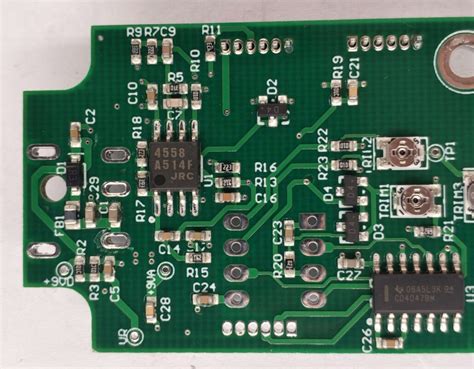
Problem 1: PCB board short circuit
This problem is one of the common faults that will directly cause the PCB board to fail to work. There are many reasons for this problem. Let’s analyze them one by one.
The biggest cause of PCB short circuit is improper pad design. At this time, the circular pad can be changed to an elliptical shape, and the distance between points can be increased to prevent short circuit.
Improper design of the direction of PCB parts can also cause the board to short circuit and fail to work. For example, if the foot of SOIC is parallel to the solder wave, it is easy to cause a short circuit accident. At this time, the direction of the part can be appropriately modified to make it perpendicular to the solder wave.
There is another possibility that can cause a short circuit fault in the PCB, that is, the automatic plug-in bent foot. Since IPC stipulates that the length of the wire pin is less than 2mm and there is a concern that the parts will fall off when the bending angle is too large, it is easy to cause a short circuit. The solder joint needs to be more than 2mm away from the circuit.
In addition to the three reasons mentioned above, there are some other reasons that can also cause short circuit failures on PCB boards, such as too large substrate holes, too low tin furnace temperature, poor board solderability, solder mask failure, board surface pollution, etc., which are all relatively common causes of failure. Engineers can compare the above reasons with the circumstances of the failure and eliminate and check them one by one.
Problem 2: Dark and granular contacts appear on the PCB board
The problem of dark or granular contacts on the PCB board is mostly due to solder contamination and too much oxide mixed in the molten tin, resulting in a too brittle solder joint structure. Be careful not to confuse it with the dark color caused by using solder with a low tin content.
Another reason for this problem is that the composition of the solder itself used in the processing and manufacturing process changes, and the impurity content is too high, so pure tin needs to be added or the solder needs to be replaced. The scar glass has a physical change in fiber layering, such as separation between layers. But this situation is not a bad solder joint. The reason is that the substrate is overheated, and the preheating and soldering temperatures need to be reduced or the substrate travel speed needs to be increased.
Question 3: PCB solder joints turn golden yellow
Generally, the solder of the PCB board is silver-gray, but occasionally there are golden solder joints. The main reason for this problem is that the temperature is too high. At this time, you only need to lower the temperature of the tin furnace.
Question 4: The board is also affected by the environment
Due to the structure of the PCB itself, it is easy to cause damage to the PCB board when it is in an unfavorable environment. Extreme temperature or temperature fluctuations, excessive humidity, high-intensity vibration and other conditions are factors that lead to reduced performance or even scrapping of the board. For example, changes in ambient temperature can cause the board to deform. Therefore, it will damage the solder joints, bend the shape of the board, or may cause the copper traces on the board to break.
On the other hand, moisture in the air can cause oxidation, corrosion and rust on metal surfaces, such as exposed copper traces, solder joints, pads and component leads. Accumulating dirt, dust or debris on the surface of components and boards can also reduce air flow and cooling of components, causing PCB overheating and performance degradation. Vibration, dropping, hitting or bending PCBs can deform them and cause cracks, while high current or overvoltage can cause PCB board breakdown or rapid aging of components and pathways.
Problem 5: PCB Open Circuit
Open circuits occur when traces are broken, or when solder is only on the pads and not on the component leads. In this case, there is no adhesion or connection between the component and the PCB. Just like short circuits, these can also occur during the production process or during soldering and other operations. Vibrating or stretching boards, dropping them or other mechanical deformation factors can damage traces or solder joints. Similarly, chemicals or moisture can cause wear of solder or metal parts, resulting in component lead breaks.
Problem 6: Loose or misaligned components
During the reflow process, small components may float on the molten solder and eventually break away from the target solder joint. Possible causes of shifting or tilting include vibration or bounce of components on soldered PCB boards due to insufficient board support, reflow oven settings, solder paste issues, human error, etc.
Problem 7: Soldering Problems
The following are some of the problems that can occur due to poor soldering practices:
Disturbed solder joints: Solder moves before solidifying due to external disturbances. This is similar to a cold solder joint, but the cause is different and can be corrected by reheating and ensuring that the solder joint is not disturbed while cooling.
Cold solder joints: This occurs when the solder does not melt properly, resulting in a rough surface and unreliable connections. Cold solder joints can also occur due to excess solder preventing complete melting. The remedy is to reheat the joint and remove excess solder.
Solder bridges: This occurs when solder crosses and physically connects two leads together. These have the potential to form unintended connections and shorts that can burn components or burn traces when current is too high.
Pads: Inadequate wetting of pins or leads. Too much or too little solder. Pads that have been lifted due to overheating or rough soldering.
Problem 8: Human Error
The majority of defects in PCB manufacturing are caused by human error. In most cases, incorrect production processes, incorrect placement of components, and unprofessional manufacturing specifications are responsible for up to 64% of avoidable product defects. The likelihood of defects increases with circuit complexity and the number of production processes due to the following reasons: densely packed components; multiple circuit layers; fine routing; surface soldered components; power and ground planes.
Although every manufacturer or assembler hopes that the PCB boards produced are free of defects, there are several design and production process problems that cause PCB board problems.
Typical problems and results include the following: poor welding can lead to short circuits, open circuits, cold solder joints, etc.; misalignment of board layers can lead to poor contact and poor overall performance; poor insulation of copper traces can lead to arcing between traces; placing copper traces too close to the path can easily lead to the risk of short circuits; insufficient thickness of the circuit board can lead to bending and breaking.
END
Disclaimer: The content of this article is authorized by 21ic and the copyright belongs to the original author. All information and storage services are provided. The article only represents the author’s personal views, not the position of this platform. If you have any questions, please contact us, thank you!
Power system design
Scan the QR code to follow more exciting content
This site statement: This article is authorized by the author or relevant institutions for the purpose of conveying more information. It does not mean that this site agrees with its views, and this site does not guarantee or promise the authenticity of the content. If you need to reprint, please contact the author of this column. If the content of the article infringes your rights, please contact this site to delete it in time.
Optimizing the EMC and efficiency of high-power DC/DC converters The secrets that I have to tell Mouser-BOM and search functions make selection and procurement smoother and more efficient Power modules that meet the requirements of 24 V industrial voltage networks Five steps to design a DC/DC switching power supply that meets electromagnetic compatibility Vehicle-mounted 36 V voltage detector with delay function IC suitable for data centers
Change a batch
Extended reading
[Communication Pioneer] Avita and Seres have invested! Huawei Yinwang may become “China’s Bosch”
On September 2, Huawei, which does not make cars, may give birth to a larger unicorn company. With the entry of Avita and Seres, Huawei Yinwang has become more and more eye-catching.
Keywords: Avita Seres Huawei
[PR Newswire Global TMT] Trianz and AWS reached a strategic cooperation agreement to completely change the way of cloud adoption and management