How to make PCB panels? What are the panel rules of PCB?
PCB is a printed circuit board. In the field of electronics, PCB is the most basic device. The main function of PCB is to make various electronic components form a connection of a predetermined circuit and play the role of relay transmission. In order to enhance everyone’s understanding of PCB, this article will introduce the PCB panel method and some PCB panel rules. If you are interested in PCB, you may wish to continue reading with the editor.
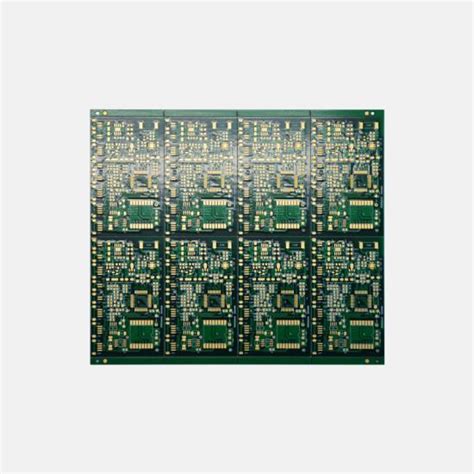
1.PCB panel method
PCB panel is just for the convenience of production. For board manufacturers, their base materials are generally large. Many boards are made at a time, and then they are cut one by one. If the panel is mainly used for welding production, imagine a fingernail-sized board welded one by one on an SMT machine as big as a car.
There are several definitions of PCB panel! Convenient customer plug-in is one, convenient manufacturer’s own production is one, and saving materials is one! Convenient plug-in means that the customer requires this kind of assembly, and you must do it as required. Convenient production for the manufacturer is convenient V cutting, etc. Saving materials is to use materials more perfectly without wasting or leaving too much scraps! For example, if you cut 34X41 CM panels for 1.2m x 1m materials, it will be perfect.
PCB panelization method, including the method of creating finished board panelization worksheet and blank board panelization worksheet by using Excel program stored in a known computer and the method of using the above worksheet; the finished board panelization worksheet is used to complete the process of same-phase and different-phase panelization of finished boards on blank boards, each column cell of the finished board panelization worksheet is used to place the same category of data of different blank board panelization schemes or the Excel internal function calculation formula of the data, and each row cell is used to place different categories of data of the same panelization scheme or the Excel internal function calculation formula of the data, and the specific method of creating the finished board panelization worksheet is as follows:
(1) Start the Excel program stored in the known computer, create a new workbook, and select a worksheet;
(2) Use a cell in the table to enter the name of the worksheet:
(3) Use a row of cells in the table as the header of the worksheet, and enter the category name of the data in its column in each cell;
(4) Create a data input area:
(5) Create a data calculation area
(6) Create a data output area
(7) Create a panel calculation area
(8) Create an indirect output area. Use Excel’s internal search and reference functions to reference all the data in the panel calculation area worksheet and place it in the indirect output area.
2.PCB panel rules
First of all, we must make it clear that in order to facilitate production, PCB circuit board panelization generally requires the design of Mark points, V-grooves, and processing edges.
(I) PCB panelization appearance design
- The border (clamping edge) of the PCB panelization method should adopt a closed-loop control design to ensure that the PCB panelization method is not easily deformed after being fixed on the fixture.
- The total width of the PCB panelization method is ≤260mm (SIEMENS line) or ≤300mm (FUJI line); if automatic gluing is required, the total width × length of the PCB panelization method is ≤125mm × 180mm.
- The appearance of the PCB panelization method should be as close to the square as possible. It is strongly recommended to use 2×2, 3×3, … panelization methods; but it is not necessary to make positive and negative boards;
(II) PCB V-groove
- After opening the V-groove, the remaining thickness X should be (1/4~1/3) the board thickness L, but the minimum thickness X must be ≥0.4mm. For boards with heavy loads, the upper limit can be used, and for boards with light loads, the lower limit can be used.
- The displacement S of the cuts on both sides of the V-groove should be less than 0.mm; due to the limitation of the minimum reasonable thickness, for boards with a thickness of less than 1.3mm, it is not suitable to use the V-groove panelization method.
(III) Mark point
- When setting the standard selection point, generally leave a 1.5mm larger unobstructed solder area around the selection point.
- Used to assist the electronic optical positioning of the SMT placement machine. There are at least two different measurement points at the top corners of the PCB with patch components. The measurement points for electronic optical positioning of a whole PCB are generally at the corresponding positions of the top corners of a whole PCB; the measurement points for electronic optical positioning of layered PCB are generally at the corresponding positions of the top corners of layered PCB.
- For QFP (square flat package) components with a wire spacing of ≤0.5mm and BGA (ball grid array package) components with a ball spacing of ≤0.8mm, in order to improve the precision of the patch, it is required to set measurement points at the two corners of the IC.
(IV) Processing edge
- There should be no large or protruding components around the edge of the panel and the internal motherboard, and the nodes between the motherboards, and the edge of the electronic components and the PCBpcb circuit board should leave more than 0.5mm of space to ensure the normal operation of the laser cutting blade.
(V) On-board positioning holes
- Standard marks used for the positioning of the entire PCB circuit board of the PCBpcb circuit board and for the positioning of fine-pitch components. Generally, QFPs with a spacing of less than 0.65mm should be set at their top corners; standard marks used for the positioning of the PCB sub-board of the panel should be used in pairs and arranged at the top corners of the positioning elements.
- Large electronic components should leave positioning columns or positioning holes, mainly such as I/O ports, microphones, battery ports, toggle switches, headphone jacks, motors, etc.
A good PCB designer should take into account the factors of manufacturing when designing a panel to ensure the purpose of convenient processing, improving productivity and reducing product costs.