Electromagnetic compatibility design of electronic equipment
1 Introduction
The widespread application and development of electronic equipment will inevitably lead to the continuous increase of the electromagnetic field level generated by them in the surrounding space. Electronic equipment will inevitably work in the electromagnetic environment.
Therefore, it is necessary to solve the adaptability of electronic equipment in the electromagnetic environment. If the electromagnetic compatibility problem of the electronic equipment system is not solved, the entire system will not work properly, so the importance of electromagnetic compatibility design of electronic equipment should be fully valued by us. The research on electromagnetic compatibility is carried out around the three elements that constitute electromagnetic interference, namely, the interference source, the interference transmission path and the interference receiver.
The electromagnetic compatibility design of electronic equipment mainly includes: limiting the electromagnetic emission of the interference source, controlling the propagation of electromagnetic interference and enhancing the anti-interference ability of sensitive equipment.
2 Electromagnetic compatibility of electronic equipment
Electromagnetic compatibility refers to the ability of a device, equipment or system to operate well in the electromagnetic environment in which it is located and not to produce any unbearable electromagnetic disturbance to the environment in which it is located. Electromagnetic compatibility covers electromagnetic interference and electromagnetic sensitivity. In order to achieve non-interference and compatible operation of the equipment in the system, it is necessary to control the electromagnetic emission of the interference source and improve the anti-interference degree of the disturbed object.
The basis for electromagnetic compatibility design is the electromagnetic environment in the system and the electromagnetic sensitivity of the equipment in the system. Assume that the power of the interference source N in the system is Pn (n=1, 2, …), and the tolerance of electromagnetic interference that the interfered device M can withstand is Pm (m=1, 2, …), then the interference power Pamn can be determined by the following formula:
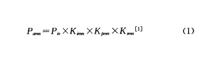
Where: Kmn is the effective effect coefficient of the interference source N on the interfered source device M; Kpmn is the coupling effect coefficient of the interference source N on the interfered source device M; Kmn is the sensitivity of the interfered source device M to electromagnetic interference.
When the interference power Pamn is greater than the tolerance Pm of the interfered device, measures need to be taken to improve electromagnetic compatibility.
When Pamn>Pm, measures can be taken to reduce the interference source power Pm or reduce the effective interference component of the interference source on the interfered device M (i.e. reduce Kmn). Measures can also be taken to reduce the coupling coefficient Kpmn of the interference source N on the interfered device M, such as reducing the coupling capacitance, reducing the coupling inductance or cutting off the coupling channel of the common impedance; measures can also be taken to reduce the electromagnetic interference sensitivity Kmn of the interfered device M or increase the interference tolerance Pm of the interfered device.
3 Electromagnetic interference mode and propagation path
Electromagnetic interference can be divided into natural interference source and artificial interference source according to the interference source. Both forms of electromagnetic interference are the main factors affecting the electromagnetic compatibility of electronic equipment. At the same time, clarifying the energy and propagation path of electromagnetic interference is a major research content of the electromagnetic compatibility design of electronic equipment.
3.1 Internal Interference
Internal interference refers to the mutual interference between components inside electronic equipment, mainly including the following situations:
1) Interference caused by leakage of the working power supply through the distributed capacitance and insulation resistance of the line;
2) Interference caused by mutual coupling of signals through the impedance of the ground wire, power supply and transmission wire or mutual inductance between wires;
3) Interference caused by heating of certain components inside the equipment or system, affecting the stability of the components themselves or other components;
4) Interference caused by magnetic fields and electric fields generated by high-power and high-voltage components affecting other components through coupling.
3.2 External interference
External interference refers to the interference caused by factors outside the electronic equipment or system to the line, equipment or system, mainly including the following situations:
1) Interference caused by external high voltage and power supply to the line, equipment or system through insulation leakage;
2) External high-power equipment generates a strong magnetic field in space, which interferes with the electronic circuit, equipment or system through mutual coupling;
3) Interference caused by external electromagnetic waves in space to the electronic circuit, equipment or system;
4) Interference caused by unstable working environment temperature, which causes changes in the parameters of components inside the electronic circuit, equipment or system;
5) Interference caused by equipment powered by the industrial power grid and by the grid voltage through the power transformer.
3.3 Transmission path of electromagnetic interference
1) Electromagnetic interference transmitted along the power line or signal line is called conducted interference. There are various connections between the devices in the electronic system or between the units in the electronic equipment. Such as power lines, signal interconnection lines and common ground lines, etc., so it is possible to transmit the electromagnetic energy of a device (or unit circuit) along such wires to adjacent devices or unit circuits, causing interference;
2) Radiated interference refers to electromagnetic interference propagated through space.
The space around the disturbance source can be divided into two areas: the area close to the disturbance source is called the near field area or the induction field area; the area with a distance greater than λ/(2π) is called the far field area or the radiation field area.

4 Electromagnetic compatibility design
The interference source, coupling path and receptor (sensitive device) constitute the three elements of electromagnetic interference, and none of them can be missing. The purpose of electromagnetic compatibility design of electronic equipment is to enable electronic equipment to suppress various external interferences, so that electronic equipment can work normally in a specific electromagnetic environment, and at the same time reduce the electromagnetic interference of electronic equipment itself to other electronic equipment. The content of electromagnetic compatibility design includes: limiting the electromagnetic emission of interference sources, controlling the propagation of electromagnetic interference and enhancing the anti-interference ability of sensitive equipment.
4.1 PCB design
PCB is the cornerstone of electronic equipment, and the electromagnetic compatibility design of PCB is the cornerstone of electromagnetic compatibility design of equipment. When designing PCB, measures are mainly taken in terms of suppressing conduction and radiation to reduce the impact of electromagnetic interference. The key to the electromagnetic compatibility design of electronic equipment PCB lies in the inherent electromagnetic sensitivity characteristics of analog and logic active devices. Since square wave signals have high-order harmonic components, when designing digital circuits, low edge change speeds should be selected as much as possible while meeting product design requirements. In addition to component selection, effective means such as decoupling capacitors, ferrite terminations, line layout, ground and power supply design should be used to enhance decoupling effects and optimize anti-interference performance.
4.2 Shielding Design
Shielding is a measure that uses shielding bodies to prevent or reduce electromagnetic energy transmission. The shielding body is a barrier layer that is used to block or reduce electromagnetic energy transmission and seal or shield the device. It can be conductive, magnetic, dielectric, or with non-metallic absorption fillers. Under the premise that the components and layout of the equipment are certain. Shielding becomes a very important content in electromagnetic compatibility design. When designing shielding, focus on the following measures:
1) Selection of shielding body materials. Shielding materials are mainly divided into electrical shielding and magnetic shielding. When designing electromagnetic compatibility, shielding materials should be reasonably selected according to the specific use environment of the equipment. The relative conductivity σr and relative magnetic permeability ur of commonly used metal materials are shown in Table 1.
2) Electromagnetic shielding design of gaps. Practice has shown that when the maximum linear dimension of the gap is equal to an integer multiple of the half wavelength of the interference source, the electromagnetic leakage of the gap is the largest. Generally, the maximum linear dimension of the gap is required to be less than λ/100 wavelength, or at least not greater than λ/10 wavelength. The structural schematic diagram and equivalent circuit of the gap are shown in Figure 1. In engineering design, in order to reduce the length of the gap, the following designs are mainly adopted:
(1) Reasonable arrangement of screws;
(2) Shielding design using conductive flexible media;
(3) Shielding design with increased contact surface.
Table 1 Relative conductivity σr and relative magnetic permeability ur of commonly used metal materials to copper
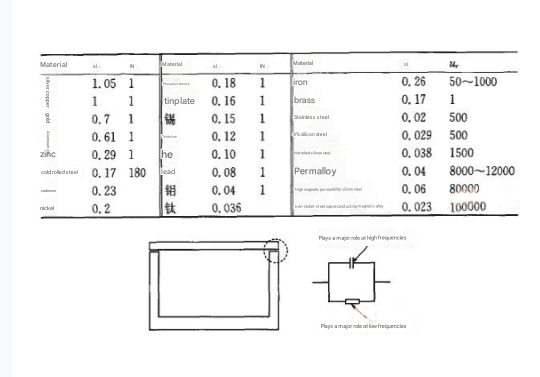
Figure 1 Schematic diagram of gap and its equivalent circuit diagram
3) Electromagnetic shielding design of holes. Electronic equipment will inevitably have some holes due to ventilation and heat dissipation, control shaft, meter head installation and connecting cables. The leakage of electromagnetic energy through the holes is one of the important reasons for the decline in the shielding effectiveness of the shielding body. And the shielding effect will become smaller as the hole increases. Generally speaking, the size of the hole should be less than λ/50 and not greater than λ/20.
4.3 Grounding technology
In electronic equipment, grounding is an important means to suppress electromagnetic noise and prevent interference, including the selection of grounding points, the design of circuit combination grounding and the application of grounding interference suppression measures. The following are grounding technology designs adopted to reduce electromagnetic interference:
1) Reduce the potential difference between grounding points;
2) Tubular grounding wire;
3) Ensure the electrical connection reliability of the grounding wire;
4) Choice of grounding method. There are three basic grounding methods in electronic equipment: floating ground, single-point grounding and multi-point grounding. Single-point grounding is suitable for low frequency, and multi-point grounding is suitable for high frequency. Generally speaking. Single-point grounding can be used for frequencies below 1MHz, multi-point grounding should be used for frequencies above 10MHz, and mixed grounding can be used for frequencies between 1MHz and 10MHz.
4.4 Filtering technology
Filtering technology is one of the main means to suppress conducted interference of electrical and electronic equipment, and it is also an important measure to improve the ability of electronic equipment to resist conducted interference. Electromagnetic interference filters can significantly reduce the level of conducted interference and use the impedance mismatch principle to attenuate electromagnetic interference signals. The installation of the filter has a great impact on its performance. When using the filter, the following matters should be noted:
1) The metal shell of the filter must ensure good surface contact with the chassis shell, and the ground wire must be well defined;
2) The input and output lines of the filter must be kept apart and must not be parallel to avoid reducing the efficiency of the filter;
3) It is best to use twisted pair cables for the connection line of the filter, which can effectively eliminate some high-frequency interference signals;
4) The installation location of the filter should be selected at the power inlet to shorten the length of the input line in the chassis and reduce radiation interference.
4.5 Reasonable layout
Reasonable layout includes the relative position and cable routing between the units in the system. The basic principle is to keep the sensor and the interference source as far away as possible, properly separate the output and input ports, and lay high-level cables and pulse leads separately from low-level cables. Through reasonable layout, mutual interference can be reduced to a minimum without much cost.
5 Electromagnetic compatibility pre-assessment and modeling
5.1 Electromagnetic compatibility pre-assessment
The management and planning of electromagnetic compatibility are often not included in the design of electronic equipment or systems. The current popular practice is to rely on traditional design practices, and after the design is completed, pay a higher price to solve the electromagnetic interference problems that occur in the test. However, with the increasing scope and degree of electromagnetic interference problems, traditional design practices can no longer always meet the requirements of electromagnetic compatibility, and electromagnetic compatibility pre-assessment technology must be adopted.
Electromagnetic compatibility pre-assessment should be considered as early as possible during the design of equipment, subsystems or systems, and then continuously improved in subsequent designs. The main purpose of electromagnetic compatibility pre-assessment can be summarized as one or more of the following: expose problematic areas as early as possible, and make the design more economical based on this; shorten the cycle of equipment to market, etc.
5.2 Electromagnetic compatibility computer modeling
Electromagnetic compatibility is a very complex and multidisciplinary emerging discipline. In order to pre-assess the electromagnetic compatibility of a device or system, the device or system must first be simplified into a relatively simple mathematical model. Modeling methods are usually mainly restricted by frequency and modeled geometry. Using computer programs to assist electromagnetic compatibility analysis can not only save a lot of time, but also minimize calculation errors and speed up the calculation process. The computer modeling process mainly consists of the following five steps:
1) Definition of geometric description;
2) Definition of electrical description;
3) Validity of the model;
4) Definition of solution description;
5) Output display.
Regardless of the type of program used, it is essential to compare the calculation results with the actual measurement results or the results obtained based on engineering experience to check their consistency.
6 Conclusion
Electronic equipment should be fully considered and implemented in all stages of the design process, practical application and maintenance to achieve effective electromagnetic compatibility control strategies for electronic equipment. Scientific and advanced electromagnetic compatibility engineering management is an important part of effective control technology. Various interferences are random during the operation of electronic equipment. They should be pre-evaluated before design. During the design process, shielding, filtering, grounding and reasonable layout technologies should be reasonably used. The electromagnetic compatibility of the equipment should be tested through scientific experiments to locate and eliminate various interferences.