High-speed FPGA-based PCB design technology
It would be wonderful if high-speed PCB design could be as simple as connecting schematic nodes and as beautiful as what you see on a computer monitor.
However, unless the designer is new to PCB design or is extremely lucky, actual PCB design is usually not as easy as the circuit design they are engaged in. Before the design can finally work properly and someone can confirm the performance, the PCB designer faces many new challenges.
This is the current situation of high-speed PCB design-design rules and design guidelines are constantly evolving, and if they are lucky, they will form a successful solution.The vast majority of PCBs are the result of cooperation between schematic designers who are proficient in the working principles and interactions of PCB components and the various data transmission standards that constitute the input and output of the circuit board, and professional layout designers who may know a little or even nothing about what will happen after the small schematic connection is converted into printed circuit copper wire.
Usually, it is the schematic designer who is responsible for the success or failure of the final circuit board. However, the more the schematic designer knows about good layout techniques, the more opportunities there are to avoid major problems.
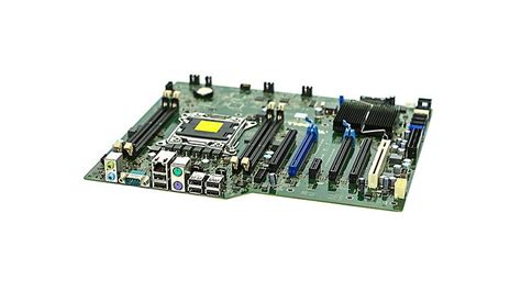
If the design contains a high-density FPGA, there are likely to be many challenges in front of the carefully designed schematic.
Hundreds of inputs and outputs, operating frequencies exceeding 500MHz (and possibly higher in some designs), and solder ball pitches as small as half a millimeter all lead to unwanted interactions between design elements.
Concurrent Switching Noise
The first challenge is likely to be what is known as concurrent switching noise (SSN) or concurrent switching outputs (SSO). A large amount of high-frequency data flow will cause problems such as ringing and crosstalk on the data line, and ground bounce and power noise problems will also appear on the power and ground planes, affecting the performance of the entire circuit board.
To solve the ringing and crosstalk on high-speed data lines, switching to differential signals is a good first step
. Since one line on the differential pair is the absorbing (Sink) end and the other provides source current, the inductive effect can be fundamentally eliminated. When using differential pairs to transmit data, since the current is kept local, it helps to reduce the “bounce” noise generated by the inductive current in the return path.
For radio frequencies up to hundreds of MHz or even GHz, signal theory shows that the maximum signal power can be transmitted when the impedance is matched. When the transmission line is not well matched, reflections will occur, and only part of the signal will be transmitted from the transmitter to the receiver, while the rest will bounce back and forth between the transmitter and the receiver. The quality of differential signal implementation on the PCB will play a big role in impedance matching (and other aspects).
Differential trace design
Differential trace design is based on the principle of impedance controlled PCB. Its model is a bit like coaxial cable. On an impedance controlled PCB, the metal plane layer can be used as a shield, the insulator is the FR4 laminate, and the conductor is the signal trace pair (see Figure 1).
The average dielectric constant of FR4 is between 4.2 and 4.5. Since the manufacturing error is unknown, it is possible to over-etch the copper line, which will eventually cause impedance errors.
The most accurate way to calculate the impedance of PCB traces is to use a field analysis program (usually in 2D, sometimes in 3D), which requires directly solving Maxwell’s equations for the entire PCB batch using finite elements. The software can analyze EMI effects based on trace spacing, line width, line thickness, and the height of the insulation layer.
100Ω characteristic impedance has become the industry standard value for differential connecting lines.
A 100Ω differential line can be made with two 50Ω single-ended lines of equal length. As the two traces are close to each other, the field coupling between the lines will reduce the differential impedance of the lines. In order to maintain the impedance of 100Ω, the width of the trace must be reduced a little. As a result, the common-mode impedance of each line in the 100Ω differential line pair will be slightly higher than 50 ohms.
In theory, the size of the trace and the material used determine the impedance, but vias, connectors and even device pads will introduce impedance discontinuities in the signal path. It is usually impossible to do without these things. Sometimes, for more reasonable layout and routing, it is necessary to increase the number of PCB layers or add features such as buried vias. Buried vias only connect part of the PCB layer, but while solving the transmission line problem, it also increases the cost of board production. But sometimes there is no choice at all. As signal speeds get faster and space gets smaller, additional demands such as buried vias begin to increase, and these should become cost factors of PCB solutions.

When stripline routing is used, the signal is sandwiched by FR-4 material. With microstrip, a conductor is exposed to the air.
Because air has the lowest dielectric constant (Er = 1), the top layer is best suited for routing critical signals such as clock signals or high-frequency SERial-to-serial (SERDES) signals. Microstrip routing should be coupled to the ground plane below, which reduces electromagnetic interference (EMI) by absorbing some of the electromagnetic field lines. In stripline, all electromagnetic field lines are coupled to the reference planes above and below, which greatly reduces EMI. If possible, try not to use wide-side coupled stripline designs. This structure is susceptible to differential noise coupled in the reference plane. In addition, balanced PCB manufacturing is required, which is difficult to control. In general, it is relatively easy to control the spacing between lines on the same layer.
Decoupling and bypass capacitors
Another important aspect that determines whether the actual performance of the PCB meets expectations needs to be controlled by adding decoupling and bypass capacitors.
Adding decoupling capacitors helps reduce the inductance between the power and ground planes of the PCB and helps control the impedance of signals and ICs everywhere on the PCB. Bypass capacitors help provide a clean power supply (provide a charge reservoir) to the FPGA. The traditional rule is to place decoupling capacitors wherever it is convenient to route the PCB, and the number of FPGA power pins determines the number of decoupling capacitors. However, the ultra-high switching speed of FPGAs completely breaks this stereotype.
In a typical FPGA board design, the capacitors closest to the power supply provide frequency compensation for the current changes of the load. Large decoupling capacitors are used to provide low-frequency filtering and prevent power supply voltage drops. The voltage drop is due to the lag in the response of the regulator when the design circuit starts. This large capacitor is usually an electrolytic capacitor with good low-frequency response, and its frequency response range is from DC to several hundred kHz.
Each FPGA output change requires charging and discharging the signal line, which requires energy.
The function of the bypass capacitor is to provide local energy storage over a wide frequency range. In addition, a small capacitor with very small series inductance is required to provide high-speed current for high-frequency transients. The slow-reacting large capacitor continues to provide current after the energy of the high-frequency capacitor is consumed.
The large number of current transients on the power bus increases the complexity of FPGA design.
Such current transients are usually related to SSO/SSN. Inserting a capacitor with very small inductance will provide local high-frequency energy, which can be used to eliminate switching current noise on the power bus. This decoupling capacitor, which prevents high-frequency current from entering the device power supply, must be very close to the FPGA (less than 1cm). Sometimes many small capacitors are connected in parallel to act as local energy storage for the device and quickly respond to changes in current demand.
In general, the routing of decoupling capacitors should be extremely short, including the vertical distance in the vias. Even a small increase will increase the inductance of the wire, thereby reducing the effectiveness of decoupling.
Other Techniques
As signal speeds increase, it becomes increasingly difficult to easily transmit data on the board. Several other techniques can be used to further improve the performance of the PCB.
The first and most obvious method is simple device layout.
Designing the shortest and most direct path for the most critical connection is common sense, but don’t underestimate this. Why bother to adjust the signal on the board when the simplest strategy can get the best results?
Almost as simple is to consider the width of the signal line.
When the data rate reaches 622MHz and even higher, the skin effect of signal transmission becomes more and more prominent. When the distance is long, a very thin trace (such as 4 or 5 mil) on the PCB will form a large attenuation to the signal, just like a low-pass filter with poor attenuation that is not designed well, and its attenuation increases with frequency. The longer the backplane is and the higher the frequency is, the wider the signal line should be. For backplane traces longer than 20 inches, the line width should reach 10 or 12 mils.
Usually, the most critical signal on the board is the clock signal.
When the clock line is too long or poorly designed, it will amplify jitter and offset downstream, especially when the speed increases. Avoid using multiple layers to transmit the clock and do not have vias on the clock line, because vias will increase impedance changes and reflections. If the clock must be routed on the inner layer, the upper and lower layers should use ground planes to reduce delays. When the design uses FPGA PLL, noise on the power plane will increase PLL jitter. If this is critical, a “power island” can be created for the PLL. This island can use thicker etching in the metal plane to isolate the PLL analog power and digital power.
For signals with speeds exceeding 2Gbps, more expensive solutions must be considered.
At such high frequencies, backplane thickness and via design have a significant impact on signal integrity. Backplane thicknesses of 0.200 inches or less work well.
When high-speed signals are on a PCB, the number of layers should be kept to a minimum to limit the number of vias.
In thick boards, vias connecting signal layers are long and will form transmission line branches on the signal path. Buried vias can solve this problem, but the manufacturing cost is high. Another option is to use low-loss dielectric materials such as Rogers 4350, GETEK, or ARLON. These materials can cost nearly double the cost of FR4 materials, but sometimes this is the only option.
There are other design techniques for FPGAs that can provide some choices in I/O location. In critical high-speed SERDES designs, SERDES I/Os can be isolated by reserving (but not using) adjacent I/O pins. For example, a 3×3 or 5×5 BGA ball area can be reserved relative to SERDES Rx and Tx, VCCRX# and VCCTX#, and ball locations. Or if possible, keep the entire I/O bank close to the SERDES. If there are no I/O constraints in the design, these techniques can provide benefits without adding cost.
Finally, and one of the best approaches is to refer to the reference boards provided by the FPGA manufacturer. Most manufacturers will provide source layout information for the reference boards, although you may need to request it due to proprietary information. These boards usually contain standard high-speed I/O interfaces because the FPGA manufacturer needs them when characterizing and qualifying their devices. However, keep in mind that these boards are usually designed for multiple purposes and may not match the specific design requirements exactly. Even so, they can still serve as a starting point for creating a solution.
Conclusion
Of course, this article only touched on some basic concepts. Any of the topics covered here could take up the length of an entire book. The key is to understand what the goals are before investing a lot of time and effort in PCB layout design. Once the layout is completed, it will cost a lot of time and money to redesign even if the width of the trace is slightly adjusted. PCB layout engineers cannot be relied upon to produce a design that meets the actual needs. The schematic designer is always there to provide guidance, make smart choices, and take responsibility for the success of the solution.