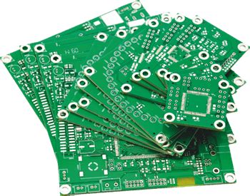
How to design RF and digital-analog circuits on the same PCB?
The popularity of handheld wireless communication devices and remote control devices is driving a significant increase in the demand for mixed analog, digital and RF designs. Handheld devices, base stations, remote controls, Bluetooth devices, computer wireless communications, many consumer electronics, and military/aerospace systems now require RF technology.
For many years, RF design has required professional designers using specialized design and analysis tools.
Typically, the RF portion of a PCB is designed by RF professionals in a separate environment and then merged with the rest of the mixed-technology PCB. This process is inefficient and often requires iterative design and the use of multiple, unrelated databases in order to integrate with hybrid technologies.
In the past, design functions were performed and duplicated in two design environments, connected by a non-intelligent ASCII interface (Figure 1(a)). The PCB system design and RF dedicated design systems in both environments have their own libraries, RF design databases and design archives. This requires that design data (schematic and layout) and libraries in both environments be managed and synchronized through a cumbersome ASCII interface.

Under this old approach, RF designers developed RF circuits in isolation from the rest of the PCB system design.
The RF circuit is then translated into the overall PCB design using an ASCII file, creating both the schematic and the physical implementation on the main PCB. If there is a problem with the RF circuit, the design must be corrected in the separate RF solution and then re-translated into the main PCB.
RF simulators only simulate ideal RF circuits.
In actual hybrid system implementations, there are many fragmented ground planes, ground planes, and adjacent RF circuits, which makes analysis very difficult, and everyone knows that these additional shapes will have a long-term impact on the operation of the RF circuits.
This old approach has been used successfully for mixed-signal board design for many years, but as the RF content of products has increased, the problems caused by two independent design systems have begun to affect designers’ productivity, time to market and product quality. quality.
To address these issues, Mentor Graphics has developed a dynamic link technology that integrates PCB schematic and layout tools with RF design and simulation tools, resulting in a new solution that overcomes traditional The shortcomings of RF design.

RF aware PCB design
To maintain design intent between PCB and RF designs, RF design tools must understand the layer-oriented structure in PCB layout, and PCB systems must understand the parameterized planar microwave components used in the RF design environment.
Another key issue is that the PCB system layouts the RF circuits into short circuits, which prevents proper design rule checking (DRC) of the design. For today’s complex RF system designs, functional RF-aware DRC is a must for design methodology to ensure correct design.
All of this helps maintain design intent. Preserving design intent is critical as it is the basis for enabling multiple round trips of design data between toolsets without loss of information.
RF design is an iterative process that requires many steps to adjust and optimize the design. In the past, RF design was very difficult in the context of real PCB design. When an optimized RF module is implemented on a PCB, there is still no guarantee that it will still work optimally. As a verification, an electromagnetic field analysis (EM) of the PCB implementation is required.


