Understanding BGA PCB Assembly: A Comprehensive Guide

Key Takeaways
The BGA PCB assembly process represents a critical advancement in the realm of electronics manufacturing. By utilizing Ball Grid Array (BGA) technology, manufacturers can achieve higher density interconnections and enhanced performance in electronic designs. One of the primary benefits of pcb assembly through BGA is the reduction in the space required for components, allowing for more compact and efficient designs. Furthermore, the connection reliability significantly improves due to the uniform distribution of solder balls that provide excellent thermal and electrical conductivity.
However, mastering pcba entails navigating through various challenges such as accurate placement, soldering issues, and inspection difficulties. To mitigate these risks, adopting strict best practices becomes essential. This includes utilizing advanced tools for alignment and ensuring proper soldering techniques to avoid defects.
"Emphasizing quality control during every phase of assembly can lead to more reliable products in the long run."
Generally, keeping abreast of the latest trends in BGA PCB manufacturing will enable professionals to implement cutting-edge solutions and remain competitive in a fast-evolving industry. Consistently updating knowledge about tools and techniques ensures that practitioners harness the full potential of pcb assembly, ultimately reflecting positively on both performance and innovation.
| Key Aspect | Importance |
|---|---|
| Component Density | Enables compact designs |
| Connection Reliability | Enhances durability |
| Quality Control | Reduces defects and improves performance |
| Technological Advancements | Keeps manufacturers competitive |
Through understanding these key takeaways, professionals can make informed decisions that elevate their expertise in BGA technology while enhancing their capacity to deliver high-quality electronic solutions.

Introduction to BGA PCB Assembly
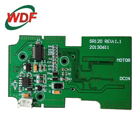
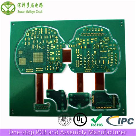
BGA PCB assembly, or Ball Grid Array printed circuit board assembly, is a sophisticated process that has gained prominence in the realm of modern electronics. This technique is characterized by the arrangement of solder balls on the underside of the component, allowing for a large number of pins to be densely packed within a small footprint. One of the primary advantages is the improved thermal and electrical performance it offers compared to traditional package types. Additionally, BGA technology facilitates pcb assembly processes that enhance solder joint reliability. The intricate nature of pcba necessitates precision in handling and placement, as even minor misalignments can lead to failed connections or performance issues. Understanding this technology is crucial for professionals and enthusiasts alike, as it serves as the backbone for various high-performance applications, including telecommunications and computing devices. The continuous evolution in design techniques and materials used in BGA assemblies also underscores its significance in driving forward innovation within electronics manufacturing.
Key Techniques in BGA PCB Assembly
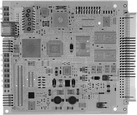
The BGA PCB assembly process is pivotal in achieving high performance and reliability in modern electronic devices. One of the fundamental techniques is solder paste application, where precise amounts of solder paste are printed onto the PCB pads where the BGA packages will be placed. This step is critical since inadequate solder paste can lead to poor joint formation, while excessive paste can cause bridging between pins. Following this, precise alignment and placement of the BGA components on the printed circuit board (PCB) are essential. Automated pick-and-place machines are often employed to ensure that each component is positioned accurately on the solder paste, reducing the risk of human error and increasing production efficiency.
Subsequently, the reflow soldering technique is utilized to form strong electrical connections. This involves heating the entire assembly to allow the solder to melt and then cooling it to solidify, creating robust joints between the BGA package and PCB pads. Careful control of temperature profiles during this process guarantees that all components achieve optimal soldering without damaging sensitive parts.
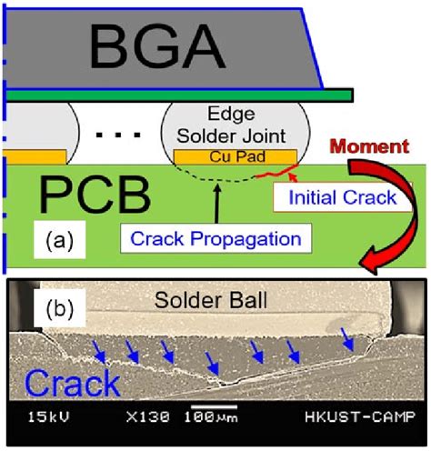
Additionally, X-ray inspection plays a crucial role in verifying solder joint integrity post-assembly. This non-destructive testing method reveals hidden defects that may not be visible externally, such as voids or insufficient wetting of solder joints. By employing these advanced techniques, professionals in pcb assembly can enhance production quality and reduce long-term failures in electronic devices, making BGA technology a preferred choice for high-density applications in various industries. Thus, understanding these key techniques can significantly advance one’s expertise in pcba processes.
Benefits of Using BGA Technology
The use of Ball Grid Array (BGA) technology in PCB assembly offers a myriad of advantages that cater to the evolving demands of modern electronics manufacturing. One significant benefit is the enhanced performance through improved electrical connectivity. BGAs allow for a greater number of interconnections in a compact space, which is essential for high-density circuit designs. This configuration contributes to lower inductance and resistance, ultimately resulting in superior signal integrity and reduced electromagnetic interference.
Moreover, the design flexibility afforded by BGA technology facilitates more efficient heat dissipation as compared to traditional packaging methods. The BGA layout allows for a larger surface area that can efficiently disperse heat away from sensitive components, ensuring reliable operation even under heavy loads. This characteristic is particularly valuable in applications where thermal management is crucial.
In addition to performance advantages, BGA PCB assembly is also known for its cost-effectiveness in large-scale production. While initial setup costs may be higher due to specialized machinery and handling processes, the scalability of production often leads to reduced per-unit costs over time. This efficiency makes pcba with BGA technology an attractive option for manufacturers aiming for both quality and affordability.
Furthermore, the automated processes used in BGA assembly, such as reflow soldering, significantly enhance precision and consistency. This reduces the likelihood of human error during assembly and leads to higher yields with fewer defective units reaching the market. The combination of these advantages positions BGA technology as a preferred choice among professionals looking to leverage advanced techniques in their electronic designs.
Common Challenges in BGA Assembly
The process of BGA PCB assembly is not without its challenges, which can impact the efficiency and effectiveness of electronic manufacturing. One prevalent issue is the alignment and placement of BGA components. Due to their design, BGA packages often include a large array of solder balls; any misalignment during placement can lead to poor connections or even damaging short circuits. Additionally, the soldering process poses its own set of risks. In pcb assembly, achieving the right temperature profile is crucial to avoid problems like cold solder joints or solder bridging. Furthermore, technicians face challenges related to inspecting PCBA due to limited visibility of the solder joints beneath the package. Traditional visual inspection methods can be inadequate in detecting these hidden defects, thus relying on advanced techniques such as X-ray inspection becomes essential. Another significant challenge lies in managing thermal expansion differences between various materials used in assembly; mismatches can cause mechanical stress during operation, leading to potential failures over time. Addressing these issues requires a deep understanding of both electronic design and manufacturing processes, ensuring that best practices are adhered to throughout production for successful BGA PCB assembly.
Best Practices for Successful BGA PCB Assembly
When engaging in BGA PCB assembly, adhering to established best practices is crucial for ensuring both reliability and performance of the final product. One of the primary considerations is the design of the PCB assembly itself. It is essential to provide ample space for solder paste application and component placement, as this facilitates optimal solder joint formation and minimizes defects. Additionally, utilizing a well-planned thermal profile during the reflow process helps in achieving uniform heating, thereby reducing potential thermal stress that can lead to failures.
Choosing the right materials is also vital; high-quality PCBA materials can significantly enhance performance. The solder paste selected should match the type of components used, as this affects both wetting properties and mechanical strength. During the placement process, automation tools like pick-and-place machines enable precision and speed, which are beneficial when working with BGA devices known for their fine pitch.
Regular inspection through techniques such as Automated Optical Inspection (AOI) can detect defects early in the process, mitigating costly downstream issues. Furthermore, implementing an effective cleaning procedure post-assembly ensures that any residual flux or contaminants do not compromise electrical performance. By following these methods and continuously improving processes based on feedback, manufacturers can achieve higher yields and improve overall reliability in their BGA PCB assembly operations.
Tools and Equipment for BGA Assembly
In the rapidly evolving field of pcb assembly, having the right tools and equipment is crucial for achieving optimal results in BGA PCB assembly. The process requires precision and accuracy, making specialized tools indispensable. Solder paste printers are one of the most critical pieces of equipment, as they ensure that the solder paste is applied evenly across the board, promoting effective adhesion of the BGA packages. After printing, it’s essential to employ pick-and-place machines, which accurately position BGA components onto the printed circuit board (PCB). This machine must maintain a high level of accuracy to prevent misalignment, which can lead to defects.
Once the components are placed, reflow ovens play a pivotal role in melting the solder paste and establishing strong electrical connections between the PCB and BGA components. These ovens carefully control temperature profiles to ensure that both components are heated uniformly. Additionally, employing X-ray inspection systems allows for non-destructive testing of hidden joints beneath BGA packages, ensuring quality control during pcb assembly.
Moreover, hand tools such as soldering irons can be useful for touch-ups or repairs on prototype boards. Having a comprehensive toolkit that includes tweezers, flux applicators, and cleaning materials enhances productivity and ensures a high-quality outcome in each pcba project. By utilizing these sophisticated tools and equipment effectively, professionals can mitigate common challenges associated with BGA assembly while enhancing their overall assembly practices in modern electronics manufacturing.
Future Trends in BGA PCB Manufacturing
As the electronics industry evolves, BGA PCB assembly is witnessing a transformative phase driven by the demand for miniaturization, enhanced performance, and cost efficiency. One of the most significant trends is the increased integration of advanced materials that facilitate better heat dissipation and signal integrity. These innovations are crucial as devices become more powerful while maintaining a compact form factor. Additionally, the rise of internet of things (IoT) applications is pushing manufacturers towards more versatile pcba processes that can accommodate varying levels of complexity.
Automation is also playing a pivotal role in the future of BGA assembly. Automated assembly lines utilizing smart technologies not only improve precision but also reduce manufacturing time and human error, leading to higher overall efficiency. Moreover, the adoption of advanced testing techniques is expected to enhance product reliability; in particular, optical inspection methods are becoming increasingly popular for detecting potential issues in BGA connections that traditional methods might overlook.
Sustainability remains a significant focus as industries strive to reduce their environmental impact. Manufacturers are exploring green practices such as lead-free soldering and recyclable materials to align with global standards for eco-friendly production.
To remain competitive in this dynamic landscape, companies must adapt to these emerging trends and invest in research and development. By embracing innovation in BGA PCB assembly, manufacturers position themselves at the forefront of technology while meeting the ever-growing demands of consumers seeking smarter, more efficient electronic devices.
Conclusion: Advancing Your Knowledge in BGA PCB Assembly
In the rapidly evolving world of electronics, understanding BGA PCB assembly is crucial for both industry professionals and hobbyists alike. This guide has illuminated important aspects of pcb assembly, detailing the key techniques and best practices that drive success in this field. As you’ve learned, BGA technology not only enhances performance but also offers significant advantages in terms of space-saving and improved electrical connectivity. However, navigating the complexities of pcba processes can come with challenges, from alignment precision to thermal management. Staying abreast of the latest developments and trends in BGA PCB manufacturing will enable you to overcome these obstacles effectively. Moreover, utilizing the right tools and adhering to best practices will play a pivotal role in achieving desired results. As you continue to expand your knowledge, remember that the insights gained from this exploration will be invaluable as you embark on your journey through the intricate landscape of modern electronics manufacturing.
Conclusion: Advancing Your Knowledge in BGA PCB Assembly
In summary, BGA PCB assembly stands out as a pivotal technique in modern electronics manufacturing. Understanding the assimilation of Ball Grid Array (BGA) technology into the broader landscape of PCB assembly processes significantly enhances both production efficiency and product reliability. Emphasizing robust methodologies and employing advanced tools in the pcba process enables manufacturers to overcome common challenges associated with BGA technology. The shift towards this sophisticated approach reflects a growing demand for higher performance and miniaturization in electronic devices, making it essential for professionals in the field to keep abreast of evolving trends and best practices. By continually updating one’s knowledge base regarding these advancements, industry players can better position themselves to harness the full potential of BGA solutions while ensuring quality and performance standards are met. Emphasizing ongoing education and adaptation will allow for a deeper understanding of how to effectively integrate BGA assembly techniques into daily operations, ultimately leading to enhanced productivity and innovation in electronic product development.
FAQs
What is BGA PCB assembly?
BGA PCB assembly refers to the process of mounting Ball Grid Array (BGA) components onto a Printed Circuit Board (PCB). This technique is commonly used in modern pcba processes due to its ability to accommodate higher pin counts while minimizing the size of the components.
What are the key advantages of using BGA technology in PCB assembly?
One of the primary benefits of BGA technology is its superior electrical performance, as it allows for shorter electrical paths and improved signal integrity. Additionally, BGAs often provide better thermal performance and can handle higher mounting densities compared to other packaging types.
What are common challenges faced during BGA assembly?
Common challenges include difficulties in alignment, solder paste application, and reliability issues after manufacturing. Ensuring proper flattening of BGA packages and managing solder joint quality during wave soldering or reflow processes are critical to achieving successful assemblies.
What tools are essential for BGA PCB assembly?
Key tools include a high-precision stencil printer for accurate solder paste application, reflow ovens or vapor phase ovens for effective heat management, and inspection equipment such as X-ray machines to verify the integrity of solder joints.
How can I ensure best practices in BGA PCB assembly?
Utilizing proper stencil design, implementing effective thermal profiles during reflow, conducting regular maintenance on equipment, and following meticulous inspection protocols can greatly enhance the success rates in pcba involving BGAs.