Classification and selection of PCB materials
1.The FR-4 we often choose is not the name of a material
The “FR-4” we often refer to is a code for a flame-resistant material grade. It means that the resin material must be able to extinguish itself after burning. It is not a material name, but a material grade. Therefore, there are many types of FR-4 grade materials used in general circuit boards, but most of them are composite materials made of so-called four-function (Tera-Function) epoxy resin plus filler (Filler) and glass fiber.
For example, the FR-4 water-green fiberglass board and black fiberglass board we are making now have functions such as high temperature resistance, insulation, and flame retardancy. So when choosing materials, you must figure out what characteristics the materials you need to achieve. In this way, you can buy the products you need.
Flexible Printed Circuit Board (FPC) is also called flexible printed circuit board, or soft printed circuit board. Flexible printed circuit board is a product that designs and produces circuit graphics on a flexible substrate in a printed manner.
There are two main types of printed circuit board substrates: organic substrate materials and inorganic substrate materials. The most commonly used are organic substrate materials. Different PCB substrates are used for different numbers of layers. For example, 3-4 layer boards use prefabricated composite materials, while double-sided boards mostly use glass-epoxy resin materials.
2.When choosing boards, we need to consider the impact of SMT
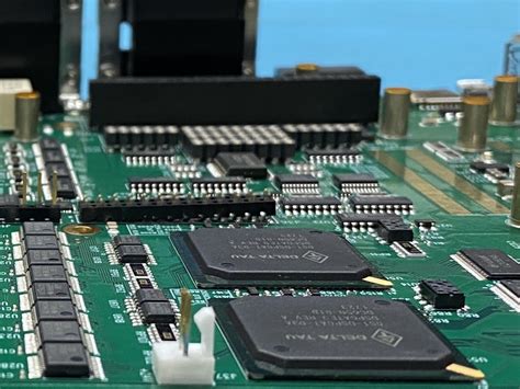
During the lead-free electronic assembly process, due to the increase in temperature, the bending degree of the printed circuit board increases when heated. Therefore, in SMT, it is required to use boards with a small bending degree as much as possible, such as FR-4 and other types of substrates. Due to the influence of the expansion and contraction stress of the substrate after heating on the components, it will cause electrode peeling and reduce reliability. Therefore, the material expansion coefficient should also be paid attention to when selecting materials, especially when the components are larger than 3.2×1.6mm. PCBs used in surface assembly technology require high thermal conductivity, excellent heat resistance (150°C, 60min) and solderability (260°C, 10s), high copper foil bonding strength (above 1.5×10⁴Pa) and bending strength (25×104Pa), high conductivity and small dielectric constant, good punching performance (accuracy ±0.02mm) and compatibility with cleaning agents. In addition, the appearance is required to be smooth and flat, without warping, cracks, scars and rust spots.
3.PCB thickness selection
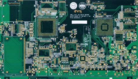
The thickness of printed circuit boards is 0.5mm, 0.7mm, 0.8mm, 1mm, 1.5mm, 1.6mm, (1.8mm), 2.7mm, (3.0mm), 3.2mm, 4.0mm, and 6.4mm. PCBs with a thickness of 0.7mm and 1.5mm are used for the design of double-sided boards with gold fingers, and 1.8mm and 3.0mm are non-standard sizes. From the production perspective, the size of the printed circuit board should not be less than 250×200mm. The general ideal size is (250~350mm)×(200×250mm). For PCBs with a long side less than 125mm or a wide side less than 100mm, it is easy to use the paneling method. The surface assembly technology stipulates that the bending amount of the substrate with a thickness of 1.6mm is ≤0.5mm for the upper warpage and ≤1.2mm for the lower warpage. The curvature usually allowed is below 0.065%. It is divided into 3 types according to metal materials, as shown in the typical PCB; it is divided into 3 types according to the hardness and softness of the structure. Electronic plug-ins are also developing towards high pin count, miniaturization, SMD and complexity. Electronic plug-ins are installed on the circuit board through pins and the pins are soldered on the other side. This technology is called THT (Through Hole Technology) insertion technology. In this way, holes need to be drilled for each pin on the PCB board, which illustrates the typical application of PCB.
4.Drilling
With the rapid development of SMT patch technology, multi-layer circuit boards need to be connected, which is ensured by electroplating after drilling, which requires various drilling equipment. In order to meet the above requirements, PCB CNC drilling equipment with different performances are currently launched at home and abroad. The production process of printed circuit boards is a complex process, which involves a wide range of processes, mainly involving photochemistry, electrochemistry, and thermochemistry; there are also many process steps involved in the production process. Take the hard multi-layer circuit board as an example to illustrate its processing procedures. Drilling is a very important process in the whole process. The processing of holes takes the longest time. The position accuracy of the holes and the quality of the hole walls directly affect the subsequent processes such as metallization and patch, and also directly affect the processing quality and cost of printed circuit boards. The principle, structure and function of CNC drilling machines. Common methods for drilling holes in circuit boards include CNC mechanical drilling methods and laser drilling methods. At this stage, mechanical drilling methods are the most commonly used.