Research on high-frequency PCB design
With the advancement of electronic technology, the complexity and application scope of PCB (printed circuit board) have developed rapidly. Designers engaged in high-frequency PCB must have the corresponding basic theoretical knowledge and rich experience in high-frequency PCB production. In other words, whether it is the drawing of the schematic diagram or the design of the PCB, it should be considered from the high-frequency working environment in which it is located, so that a more ideal PCB can be designed. This article mainly studies some problems in high-frequency PCB design based on Protel99SE from the two aspects of manual layout and wiring of high-frequency PCB.
1 Layout design
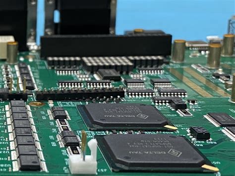
Although Protel99SE has the function of automatic layout, it cannot fully meet the working needs of high-frequency circuits. It often depends on the designer’s experience. According to the specific situation, the manual layout method is used to optimize and adjust the position of some components, and then the automatic layout is combined to complete the overall design of the PCB. The rationality of the layout directly affects the life, stability, EMC (electromagnetic compatibility) of the product. It must be considered comprehensively from the overall layout of the circuit board, the accessibility of the wiring and the manufacturability of the PCB, mechanical structure, heat dissipation, EMI (electromagnetic interference), reliability, signal integrity and other aspects.
Generally, components with fixed positions related to mechanical dimensions are placed first, followed by special and larger components, and finally small components. At the same time, the requirements for wiring should be taken into account. The placement of high-frequency components should be as compact as possible so that the wiring of signal lines can be as short as possible, thereby reducing the cross-interference of signal lines, etc.
1.1 Placement of positioning plug-ins related to mechanical dimensions
Power sockets, switches, interfaces between PCBs, indicator lights, etc. are all positioning plug-ins related to mechanical dimensions. Usually, the interface between the power supply and the PCB is placed at the edge of the PCB, and there should be a spacing of 3mm to 5mm from the edge of the PCB; the indicator light-emitting diode should be placed accurately as needed; switches and some fine-tuning components, such as adjustable inductors and adjustable resistors, should be placed near the edge of the PCB for easy adjustment and connection; components that need to be replaced frequently must be placed in a position with fewer components to facilitate replacement.
1.2 Placement of special components
High-power tubes, transformers, rectifiers and other heat-generating devices generate more heat when working in high-frequency states, so ventilation and heat dissipation should be fully considered during layout, and such components should be placed in places on the PCB where air can easily circulate. High-power rectifiers and adjustment tubes should be equipped with heat sinks and should be kept away from transformers. Heat-sensitive components such as electrolytic capacitors should also be kept away from heating devices, otherwise the electrolyte will be dried, causing its resistance to increase, performance to deteriorate, and affecting the stability of the circuit.
Components that are prone to failure, such as adjustment tubes, electrolytic capacitors, relays, etc., should also be placed for maintenance convenience. For test points that often need to be measured, care should be taken to ensure that the test rod can be easily contacted when arranging components.
Since a 50Hz leakage magnetic field is generated inside the power supply equipment, when it is connected to certain parts of the low-frequency amplifier, it will interfere with the low-frequency amplifier. Therefore, they must be isolated or shielded. It is best to arrange the amplifier stages in a straight line according to the schematic diagram. The advantage of this arrangement is that the ground current of each stage is closed and flows in this stage, without affecting the operation of other circuits. The input stage and the output stage should be as far away as possible to reduce the parasitic coupling interference between them.
Considering the signal transmission relationship between the functional circuits of each unit, the low-frequency circuit should be separated from the high-frequency circuit, and the analog circuit should be separated from the digital circuit. The integrated circuit should be placed in the center of the PCB, so that it is convenient for each pin to be connected to other devices.
Devices such as inductors and transformers have magnetic coupling, and they should be placed orthogonally to reduce magnetic coupling. In addition, they all have strong magnetic fields, and there should be a suitable large space or magnetic shielding around them to reduce the impact on other circuits.
Appropriate high-frequency decoupling capacitors should be configured at key parts of the PCB, such as a 10μF~100μF electrolytic capacitor should be connected to the input end of the PCB power supply, and a 0.01pF ceramic capacitor should be connected near the power pin of the integrated circuit. Some circuits also need to be configured with appropriate high-frequency or low-frequency chokes to reduce the impact between high and low frequency circuits. This should be considered when designing and drawing the schematic diagram, otherwise it will also affect the working performance of the circuit.
The spacing between components should be appropriate, and the spacing should take into account whether there is a possibility of breakdown or sparking between them.
For amplifiers containing push-pull circuits and bridge circuits, attention should be paid to the symmetry of the electrical parameters of the components and the symmetry of the structure when arranging them, so that the distribution parameters of the symmetrical components are as consistent as possible.
After completing the manual layout of the main components, the component locking method should be used to prevent these components from moving during automatic layout. That is, executing the Editchange command or selecting Locked in the Properties of the component can lock it and no longer move it.
1.3 Placement of ordinary components
For ordinary components, such as resistors and capacitors, the arrangement of components should be neat, the size of the occupied space, the accessibility of wiring and the convenience of welding should be considered, and the automatic layout method can be adopted.

2 Wiring design
Wiring is the overall requirement for realizing high-frequency PCB design on the basis of reasonable layout. Wiring includes two methods: automatic wiring and manual wiring. Usually, no matter how many key signal lines there are, these signal lines are first manually routed, and after the wiring is completed, the wiring of these signal lines is carefully checked. After the inspection is passed, it is fixed, and then other wiring is automatically routed. That is, a combination of manual and automatic wiring is used to complete the wiring of the PCB.
During the wiring process of high-frequency PCB, special attention should be paid to the following aspects.
2.1 Wiring Direction
It is best to use a full straight line according to the flow direction of the signal. When turning, a 45° fold line or arc curve can be used to complete it, which can reduce the external emission of high-frequency signals and mutual coupling. The wiring of high-frequency signal lines should be as short as possible. According to the operating frequency of the circuit, the length of the signal line wiring should be reasonably selected, which can reduce the distributed parameters and reduce the signal loss. When making a double-sided board, it is best to make the wiring on two adjacent layers perpendicular, oblique or curved. Avoid parallelism, which can reduce mutual interference and parasitic coupling.
High-frequency signal lines and low-frequency signal lines should be separated as much as possible, and shielding measures should be taken if necessary to prevent mutual interference. For the signal input end with relatively weak reception, it is easy to be interfered by external signals. The ground wire can be used as a shield to surround it or the high-frequency connector can be shielded. Parallel routing should be avoided on the same layer, otherwise distributed parameters will be introduced, which will affect the circuit. If it cannot be avoided, a grounded copper foil can be introduced between the two parallel lines to form an isolation line.
In digital circuits, for differential signal lines, they should be routed in pairs, and try to make them parallel, close, and not much different in length.
2.2 Wiring form
In the wiring process of PCB, the minimum width of the line is determined by the adhesion strength between the wire and the insulating layer substrate and the current intensity flowing through the wire. When the thickness of the copper foil is 0.05mm and the width is 1mm~1.5mm, 2A current can pass. The temperature will not be higher than 3℃. Except for some special routings, the width of other wiring on the same layer should be as consistent as possible. In high-frequency circuits, the spacing of the wiring will affect the size of the distributed capacitance and inductance, thereby affecting the signal loss, the stability of the circuit, and causing signal interference. In high-speed switching circuits, the spacing of the wires will affect the transmission time of the signal and the quality of the waveform. Therefore, the minimum spacing of the wiring should be greater than or equal to 0.5mm. As long as it is allowed, it is best to use a wider line for PCB wiring.
There should be a certain distance between the printed wire and the edge of the PCB (not less than the thickness of the board), which is not only convenient for installation and mechanical processing, but also improves the insulation performance.
When you encounter a line that can only be connected by a large circle during wiring, you should use flying wires, that is, directly connect with short wires to reduce the interference caused by long-distance routing.
Circuits containing magnetic sensitive components are sensitive to the surrounding magnetic field, and the corners of the wiring are prone to radiate electromagnetic waves when the high-frequency circuit is working. If a magnetic sensitive component is placed in the PCB, the wiring corner should be kept at a certain distance from it.
The wiring on the same level is not allowed to cross. For lines that may cross, you can use the method of “drilling” and “winding”, that is, let a lead “drill” through the gap under the pins of other resistors, capacitors, transistors, etc., or “wind” through one end of a lead that may cross. In special cases, if the circuit is very complex, in order to simplify the design, it is also allowed to use wire jumper to solve the crossing problem.
When the operating frequency of the high-frequency circuit is high, it is also necessary to consider the impedance matching and antenna effect of the wiring.
2.3 Wiring requirements for power lines and ground lines
According to the size of different working currents, try to increase the width of the power line. High-frequency PCBs should use large-area ground wires as much as possible and layout them at the edge of the PCB, which can reduce the interference of external signals on the circuit; at the same time, the ground wire of the PCB can be well contacted with the shell, making the ground voltage of the PCB closer to the earth voltage. The grounding method should be selected according to the specific situation. Different from the low-frequency circuit, the ground wire of the high-frequency circuit should be grounded nearby or multi-point grounding. The ground wire is short and thick to minimize the ground impedance. The allowable current requirement can reach 3 times the standard of the working current. The ground wire of the speaker should be connected to the ground point of the PCB amplifier output stage, and never arbitrarily ground.
During the wiring process, some reasonable wiring should also be locked in time to avoid repeated wiring. That is, execute the EditselectNet command and select Locked in the pre-wiring properties to lock it and no longer move it.
3 Design of pads and copper cladding
3.1 Pads and apertures
While ensuring that the minimum wiring spacing does not violate the designed electrical spacing, the pad design should be larger to ensure sufficient loop width. Generally, the inner hole of the pad is slightly larger than the lead diameter of the component. If the design is too large, it is easy to form a cold solder joint during welding. The outer diameter D of the pad is generally not less than (d+1.2) mm, where d is the inner hole diameter of the pad. For some PCBs with relatively high density, the minimum value of the pad can be (d+1.0) mm. The shape of the pad is usually set to be circular, but for the pad of the DIP packaged integrated circuit, it is best to use a runway shape, so that the area of the pad can be increased in a limited space, which is conducive to the welding of the integrated circuit. The connection between the wiring and the pad should be smoothly transitioned, that is, when the width of the wiring entering the circular pad is smaller than the diameter of the circular pad, a teardrop design should be adopted.
It should be noted that the size of the inner hole diameter d of the pad is different, and it should be considered according to the size of the actual lead diameter of the component, such as component holes, mounting holes and slot holes. The hole spacing of the pad should also be considered according to the actual installation method of the component. For example, components such as resistors, diodes, and tubular capacitors have two installation methods: “vertical” and “horizontal”, and the hole spacing of these two methods is different. In addition, the design of the pad hole spacing must also consider the minimum clearance requirements between components, especially the clearance between special components needs to be guaranteed by the hole spacing between pads.
In high-frequency PCBs, the number of vias should be minimized as much as possible, which can not only reduce the distributed capacitance but also increase the mechanical strength of the PCB. In short, in the design of high-frequency PCBs, the design of pads and their shapes, apertures and hole spacing must not only consider their particularity but also meet the requirements of the production process. The use of standardized design can not only reduce product costs, but also improve production efficiency while ensuring product quality.
3.2 Copper plating
The main purpose of copper plating is to improve the anti-interference ability of the circuit. At the same time, it is very beneficial for PCB heat dissipation and PCB strength. Copper plating grounding can also play a shielding role. However, large-area strip copper foil cannot be used, because when the PCB is used for too long, it will generate a lot of heat, and the strip copper foil is prone to expansion and falling off. Therefore, it is best to use grid-shaped copper foil when applying copper, and connect this grid with the grounding network of the circuit, so that the grid will have a better shielding effect. The size of the grid network depends on the interference frequency to be shielded.
After completing the design of wiring, pads and vias, DRC (design rule check) should be performed. The differences between the designed diagram and the defined rules are listed in detail in the inspection results, and the network that does not meet the requirements can be found. However, the DRC parameters should be set before wiring before running DRC, that is, execute the ToolsDesignRuleCheck command.
4 Conclusion
The design of high-frequency circuit PCB is a complex process, involving many factors, which may be directly related to the working performance of the high-frequency circuit. Therefore, designers need to continuously study and explore in actual work, accumulate experience, and combine new EDA (electronic design automation) technology to design a high-frequency circuit PCB with excellent performance.