Innovative Strategies for Effective HDI PCB Design Techniques
Key Takeaways
In the realm of HDI PCB design, it’s crucial to grasp the fundamentals to effectively implement innovative strategies. Understanding the key advantages of high-density interconnects can significantly streamline your projects. The versatility of HDI boards allows for a comparison of different types, each tailored for specific applications, ultimately enhancing your decision-making process. When considering the signal integrity, innovative techniques can play a pivotal role; ensure you’re aware of the latest practices that can help mitigate any potential issues. As you optimize your circuit board functionality, remember that each design tweak you incorporate may influence the overall pcb manufacturing cost significantly. Partnering with reputable pcb manufacturing companies can provide valuable insights and resources necessary for successful production. Moreover, think about how a proficient approach to pcb manufacturing business can lead to enhanced efficiency and reduced lead times in your projects.
"Stay updated with new trends in HDI technology to maintain a competitive edge in your designs."
Emphasizing these aspects will not only aid in creating an effective design but also ensure that your PCB endeavors are both innovative and economical.
Understanding the Basics of HDI PCB Design
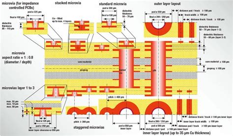
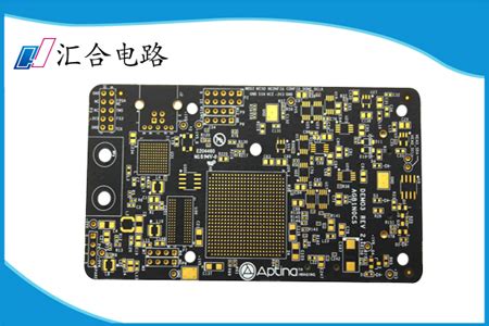
In the realm of HDI (High-Density Interconnect) PCB design, it is essential to grasp the foundational concepts that inform your approach to creating compact, efficient circuit boards. At its core, HDI PCB design leverages advanced technologies that enable the creation of intricate layouts with tightly packed interconnections. This process often employs techniques such as laser drilling and microvias, which facilitate greater connectivity in a smaller footprint. When considering PCB manufacturing, you may find that collaborating with specialized PCB manufacturing companies can significantly enhance your project outcomes by providing expertise in these advanced methods. Furthermore, understanding the PCB manufacturing cost is critical; investing in high-quality materials and technologies can lead to long-term savings by reducing the risk of failures and ensuring better product performance. Engaging in a well-planned PCB manufacturing business model will allow you to optimize your resources while navigating the increasing demand for more compact and efficient electronic solutions. By mastering these fundamentals, you set a solid foundation for your journey into more innovative design strategies and practical applications in HDI technology.
Key Advantages of High-Density Interconnects
High-Density Interconnects (HDI) in PCB design provide a variety of notable advantages that can significantly enhance the performance and functionality of modern electronics. One of the most compelling benefits is the ability to achieve greater packing density, allowing more circuitry to fit into a smaller footprint. This is particularly valuable for applications requiring compact designs, such as mobile devices and wearables. By utilizing HDI technology, you can effectively reduce the PCB manufacturing cost by minimizing the space needed for other components. Furthermore, HDI boards facilitate improved signal integrity, which is vital in applications that demand reliability and performance. The use of smaller vias and traces within HDI designs helps to lower inductance and capacitance, leading to enhanced electrical performance overall.
To better illustrate these advantages, consider the following table that outlines some key benefits associated with HDI technology compared to traditional PCB manufacturing methods:
| Advantage | HDI Boards | Traditional PCBs |
|---|---|---|
| Packing Density | High | Moderate |
| Signal Integrity | Enhanced | Lower |
| Size Reduction Potential | Significant | Limited |
| Layer Count Capability | Higher | Lower |
| Ease of Multi-layer Stack-Up | Simplified Design | Complexity Increase with Layers |
Additionally, partnering with reputable pcb manufacturing companies guarantees that you leverage state-of-the-art techniques for your projects. These companies often specialize in HDI technologies which can result in better turnaround times and higher quality products. Engaging in business models that integrate advanced design strategies further optimizes your overall project cost and efficiency. Thus, embracing HDI in your design process not only enhances functionality but also supports a more efficient and cost-effective approach to modern electronic developments.
Types of HDI Boards and Their Applications
High-Density Interconnect (HDI) boards have become increasingly significant in the realms of electronics and telecommunications. These boards utilize multiple layers of interconnects to achieve dense circuit layouts, which are essential for modern device miniaturization. You may encounter various types of HDI boards, each designed for specific applications, such as smartphones, tablets, and high-performance computing systems. In pcb manufacturing, understanding the types of HDI boards can influence decisions in choosing the right materials and layouts. For instance, you might opt for microvias in designs that require compact circuitry or choose buried vias for enhanced performance in signal integrity. Knowing the differences can also affect your budget considerations when discussing pcb manufacturing costs with different pcb manufacturing companies. These nuances are critical as they can significantly impact your project timelines, ultimately shaping a successful pcb manufacturing business approach tailored to meet client requirements while optimizing functionality and reliability in diverse applications.
Innovative Techniques for Enhancing Signal Integrity
Achieving optimal signal integrity in HDI PCB design is critical for the performance of your electronic devices. One innovative technique involves utilizing microvias, which allow for shorter signal paths and reduced parasitic capacitance. This can significantly enhance the overall signal integrity by minimizing delays and interference. In addition, implementing differential signaling can be beneficial; this method leverages paired signals to reduce electromagnetic interference, which is crucial in high-speed applications. Furthermore, by selecting appropriate materials with low dielectric constants, you can further improve signal propagation and integrity.
Moreover, as you engage with various pcb manufacturing companies, it’s essential to understand the implications of layer stacking techniques and how they influence performance. Designing with appropriate impedance control mechanisms within your HDI layout ensures that traces are optimized for the specific frequencies your device will encounter.
You should also consider the pcb manufacturing cost implications when choosing these advanced techniques; balancing high-tech designs with cost-effective solutions is key to a successful pcb manufacturing business. Striking this balance allows you to enhance signal integrity without compromising on budget or production efficiency, making your PCB designs not only innovative but also economically viable in a competitive marketplace.
Compact Circuit Board Functionality: Optimizing Design
In the world of HDI PCB design, your focus on optimizing compact circuit board functionality is crucial for achieving high performance and efficiency. A densely packed circuit board can yield remarkable advantages, such as reduced size and weight, which are essential in today’s technology-driven environment. By utilizing advanced techniques and materials, you can significantly enhance the performance of your circuit boards. For instance, integrating high-density interconnects allows for tighter trace routing while maintaining excellent signal integrity, minimizing potential loss or interference.
Additionally, you should consider the pcb manufacturing process; it plays a pivotal role in the design success. Collaborating with reputable pcb manufacturing companies is essential to ensure that your designs are produced with precision and care, thus optimizing reliability and functionality. Furthermore, understanding the pcb manufacturing cost can help you plan your project more effectively without compromising on quality. By keeping these factors in mind during design and fabrication phases, you can effectively streamline your pcb manufacturing business, leading to enhanced product outcomes and faster time to market.
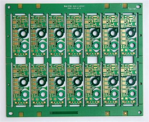
Best Practices in Fabrication and Manufacturing of HDI PCBs
When it comes to HDI PCB design, adhering to best practices during the pcb manufacturing process is crucial for maximizing the effectiveness and reliability of your circuits. Firstly, it’s essential to choose a reputable pcb manufacturing company that has extensive experience in handling high-density interconnects. These companies understand the nuances of HDI PCB fabrication and ensure that your designs are translated accurately into production. Moreover, meticulous attention to detail in the layout phase can significantly reduce the pcb manufacturing cost, as well-executed designs minimize material waste and rework.
Utilizing advanced technologies such as laser drilling and microvias not only enhances design capabilities but also optimizes space on the board without compromising performance. You should also consider implementing robust testing methods during various stages of production to ensure signal integrity and functionality, which can prevent costly defects down the line. Lastly, staying updated on emerging trends in pcb manufacturing can give you a competitive edge, allowing your projects to incorporate innovative solutions that prioritize efficiency and effectiveness. By focusing on these best practices, you will enhance the overall quality of your HDI PCBs, maintaining alignment with industry standards while optimizing your manufacturing business operations.
Future Trends in HDI PCB Technology
As you navigate the world of HDI PCB design, it’s essential to stay informed about future trends that can significantly impact your projects. One of the most promising advancements is the integration of advanced materials that enhance insulation properties and improve thermal management. This focus on material innovation not only affects the performance of high-density interconnects but can also streamline your pcb manufacturing processes. Additionally, adopting automation within pcb manufacturing companies is expected to reduce lead times and enhance production efficiency, making it easier for you to meet tight deadlines without compromising quality.
Moreover, the trend towards miniaturization in electronics necessitates innovative approaches in design and fabrication techniques. As circuits continue to shrink, utilizing microvias and blind/buried vias will become increasingly important, allowing for more compact designs while maintaining integrity and reliability. Understanding these trends is crucial in forecasting pcb manufacturing costs, as they may lead to more strategic investments in technology and equipment. Embracing these changes not only positions your projects favorably within the competitive landscape but also enhances your reputation within the evolving pcb manufacturing business environment.
In conclusion, staying ahead of these trends will empower you to leverage new opportunities within HDI PCB technology, ensuring your designs are not only cutting-edge but also cost-effective and adaptable for future market demands.
Challenges and Solutions in HDI PCB Design
When engaging in HDI PCB design, you may encounter several challenges that can impact the overall effectiveness and efficiency of your project. For instance, achieving high-density interconnects often leads to complications regarding signal integrity, due to the reduced spacing between traces and components. You’ll need to implement innovative techniques such as controlled impedance and differential signaling to mitigate these issues effectively. Additionally, the pcb manufacturing cost can escalate quickly, especially if you are not in collaboration with reputable pcb manufacturing companies. It’s essential to evaluate different pcb manufacturing business models to find solutions that align both with your budget and technical requirements.
Moreover, when working on compact circuit board functionality, maintaining thermal management becomes critical; otherwise, excessive heat can adversely affect performance. To counteract this, consider incorporating heat spreaders or thermal vias into your design. Leveraging advanced simulation tools during the initial design phase can significantly aid in predicting potential issues, enabling you to fine-tune designs before hitting the manufacturing stage. By addressing these challenges proactively, you will not only enhance the performance of your HDI PCBs but will also contribute positively to the reliability of your overall product development process.
Conclusion
In your journey towards mastering HDI PCB design, it is essential to recognize the myriad of factors influencing the effectiveness of these advanced boards. High-density interconnects are not just a trend but a necessity in today’s compact electronic solutions. When you consider PCB manufacturing, partnering with reputable pcb manufacturing companies can significantly enhance your design outcomes. These companies employ state-of-the-art technologies that facilitate robust designs while maintaining optimal signal integrity. Additionally, understanding the pcb manufacturing cost is vital; it allows you to allocate resources intelligently, ensuring that you achieve a balance between quality and affordability. As you delve deeper into the pcb manufacturing business, staying current with industry trends will empower you to implement innovative techniques that meet evolving consumer expectations. Always remember that the success of your HDI PCB projects depends significantly on how well you integrate these strategies and insights into your overall design and production process.
FAQs
What is HDI PCB design?
HDI PCB design refers to High-Density Interconnect printed circuit boards, characterized by a higher number of interconnections and smaller components, which allows for a more compact design and increased functionality.
What are the key advantages of using HDI technology?
The primary advantages include enhanced signal integrity, reduced pcb manufacturing cost, and improved thermal management. These factors make HDI PCBs ideal for applications where space and performance are critical.
How do I enhance signal integrity in high-density designs?
To enhance signal integrity, consider employing techniques such as controlled impedance routing, minimizing crosstalk through proper layout practices, and using pcb manufacturing companies that specialize in advanced technologies tailored to your specific requirements.
What types of applications benefit from HDI PCBs?
HDI PCBs are widely used in telecommunications, consumer electronics, medical devices, and automotive applications. Their compact nature supports the growing demand for sophisticated electronics within limited spaces.
What factors influence pcb manufacturing cost?
Factors influencing pcb manufacturing cost include material selection, complexity of the design, volume of production, and technology employed during the manufacturing process. It’s crucial to analyze these elements while planning your project to ensure you meet budget constraints.
How can I optimize compact circuit board functionality?
Optimizing compact circuit board functionality involves strategic placement of components, effective thermal management solutions, and utilizing multi-layer designs that accommodate both size constraints and performance requirements.